Showing Spotlights 249 - 256 of 334 in category All (newest first):
 Graphene-based nanomaterials have many promising applications in energy-related areas. In particular, there are four major energy-related areas where graphene will have an impact: solar cells, supercapacitors, lithium-ion batteries, and catalysis for fuel cells. Graphene could be a promising replacement material for indium tin oxide. A recent review provides an overview of research on graphene and its derivatives, with a particular focus on synthesis, properties, and applications in solar cells.
Oct 10th, 2013
 An increasing number of companies is involved in commercializing graphene on an industrial scale although the high cost of graphene is one of the major obstacles to its widespread adoption for commercial applications. The Nanomaterial Database we also list commercial graphene products and we keep a list of graphene manufacturers and suppliers that is constantly updated. Currently, this list contains 40 companies which are listed in this article.
Sep 19th, 2013
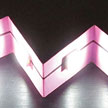 In contrast to flexible electronics, which rely on bendable substrates, truly foldable electronics require a foldable substrate with a very stable conductor that can withstand folding, i.e. an edge in the substrate at the point of the fold, which develops creases, and the deformation remains even after unfolding. That means that, in addition to a foldable substrate like paper, the conductor that is deposited on this substrate also needs to be foldable. Researchers have now demonstrated a fabrication process for foldable graphene circuits based on paper substrates.
Aug 22nd, 2013
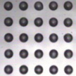 Graphene has a unique combination of properties that is ideal for next-generation electronics, including mechanical flexibility, high electrical conductivity, and chemical stability. Combine this with inkjet printing, already extensively demonstrated with conductive metal nanoparticle ink, and you get an inexpensive and scalable path for exploiting these properties in real-world technologies. Although liquid-phase graphene dispersions have been demonstrated, researchers are still struggling with sophisticated inkjet printing technologies that allow efficient and reliable mass production of high-quality graphene patterns for practical applications. Recent work has addressed these issues and proposes an approach to overcome these problems.
Aug 20th, 2013
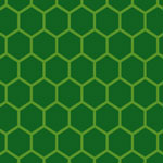
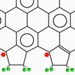 Edge magnetism is a unique property of graphene ribbons that has been predicted by theory, but not yet directly confirmed experimentally. If researchers want to utilize zigzag graphene nanoribbons (zGNRs) in spintronics, they first need to figure out a suitable termination group for zGNRs. The often used hydrogen atom termination is not a good choice since hydrogen terminated zGNRs can only be stabilized at extremely low hydrogen concentrations. In new work, researchers designed special boundaries for zGNRs that could become both stable and maintain the edge magnetism.
Jul 2nd, 2013
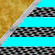 Utilization of graphene may help realize innovative low power replacements for III-V materials based high electron mobility transistors while extending operational frequencies closer to the THz regime for superior wireless communications, imaging, and other novel applications. Device architectures explored to date suffer a fundamental performance roadblock due to lack of compatible deposition techniques for nanoscale dielectrics required to efficiently modulate graphene transconductance while maintaining low gate capacitance-voltage product. In new work, researchers have shown that a double layer of graphene with structural transformation to a striped channel architecture can produce high field effect mobility at a very low operation voltage.
Jun 26th, 2013
 The low-frequency 1/f noise is a ubiquitous phenomenon found everywhere from fluctuations of human heart rates to fluctuations of electrical currents in semiconductor devices. An acceptable level of flicker 1/f noise is one of the key metrics that each new material has to pass before it can be used for practical devices. Graphene has shown a great potential for applications in high-frequency communications, analog circuits and sensors. The envisioned applications require a low level of 1/f noise, which contributes to the phase-noise of communication systems and limits the sensor sensitivity. Now, researchers have discovered a unique feature of 1/f noise in graphene, which can help understand its microscopic origin and develop new techniques for noise reduction.
May 10th, 2013
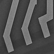
 Most of the research efforts on developing synthesis methods for graphene has focused on flat substrates. However, direct growth of graphene layers on prepatterned substrates has remained elusive. In new work, resarchers have grown graphene in prepatterned copper-coated substrates, and they apply this protocol for the fabrication of MEMS devices, in particular, atomic force microscope probes. This layer of graphene improves the functionality of the probes by making them conductive and more resistant to wear.
May 6th, 2013
 Subscribe to our Nanotechnology Spotlight feed