| Posted: May 10, 2013 |
Unusual behavior of graphene under irradiation: More damage - less noise |
| (Nanowerk Spotlight) The low-frequency 1/f noise – fluctuation process with the spectral density S∼1/fγ (where γ≈1 and f is the frequency) – is a ubiquitous phenomenon found everywhere from fluctuations of human heart rates to fluctuations of electrical currents in semiconductor devices (see our previous Nanowerk Spotlight: "Graphene helps to unravel the mystery of 1/f noise in electronic devices"). The low-frequency electronic 1/f noise was first discovered in vacuum tubes and then observed in a wide variety of electronic materials and devices. The common name for the 1/f noise, which is also known as flicker noise, in its various manifestations does not imply the common origin. |
| An acceptable level of flicker 1/f noise is one of the key metrics that each new material has to pass before it can be used for practical devices. Graphene has shown a great potential for applications in high-frequency communications, analog circuits and sensors. The envisioned applications require a low level of 1/f noise, which contributes to the phase-noise of communication systems and limits the sensor sensitivity. Despite major research efforts there is still no conventionally accepted model for physical mechanisms behind 1/f noise in graphene. Correspondingly, no comprehensive methods for 1/f noise suppression in graphene devices have been developed. |
| Now, a team of researchers from the University of California – Riverside (UCR), Rensselaer Polytechnic Institute (RPI) and Ioffe Physical-Technical Institute of The Russian Academy of Sciences, have discovered a unique feature of 1/f noise in graphene, which can help understand its microscopic origin and develop new techniques for noise reduction. |
| The researchers found that 1/f noise in graphene reduces with increasing concentration of defects induced by irradiation. In most of other materials and devices the electronic 1/f noise increases with increased concentration of structural and other defects. |
| The team of researchers led was by Dr. Alexander A. Balandin, Professor of Electrical Engineering and Founding Chair of Materials Science and Engineering at UCR and included Dr. Md. Zahid Hossain, Research Associate in Professor Balandin’s Nano-Device Laboratory (NDL), Dr. Michael S. Shur, Patricia W. and C. Sheldon Roberts Professor of Solid State Electronics at RPI and Dr. Sergey Rumyantsev, Research Professor at RPI and Ioffe Institute. |
| The results of this research have recently appeared in the Applied Physics Letters under the title “Reduction of 1/f noise in graphene after electron-beam irradiation”. The pre-print is available at arXiv. |
| The team found that bombardment of graphene devices with relatively low energy electrons (20 keV of energy) can reduce the normalized noise spectral density by an order-of magnitude at the radiation dose of 104 µC/cm2 (see Figure 1). |
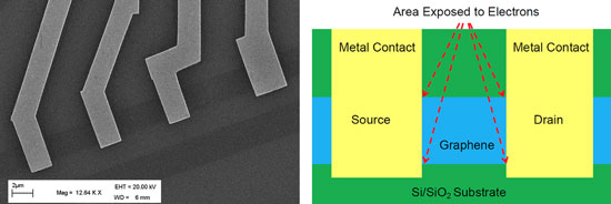 |
| Figure 1: Graphene device irradiation with electron beams. (a) SEM image of graphene devices with multiple metal contacts. The dark ribbons are graphene channels while the white regions are Ti/Au (10nm/90nm) electrodes. The scale bar is 2 µm. (b) Schematic of the irradiation process showing the area exposed to the electron beam. The whole area between the metal contacts is irradiated. The devices were fabricated by Dr. Md. Zahod Hossain at UC Riverside. (The image is courtesy of Prof. Alexander A. Balandin) |
| "We planned these experiments in order to see how strongly 1/f noise level will change with increasing defect concentrations," explains Balandin. "The defects were introduced by electron beam irradiation. Similar studies were previously carried out for other material systems and were important in understanding the noise characteristics. I was very much surprised with the results of the measurements. The noise was not increasing but rather decreasing with increasing radiation dose. I asked my group members at UC Riverside to fabricate more graphene devices and repeat the measurements many times. The whole project took more than a year. The emasurements gave reproducible results." |
| The observed 1/f noise reduction in graphene is illustrated in Figure 2: |
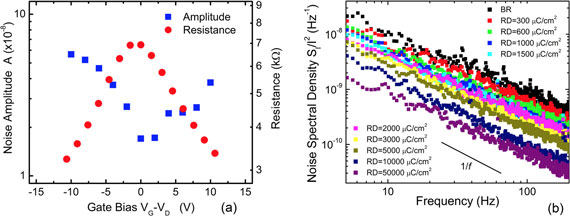 |
| Figure 2: Noise suppression in graphene via electron beam irradiation. (a) Noise amplitude A as the function of the gate bias and channel resistance in pristine graphene. (b) Noise spectral density, SI/I2, as a function of frequency for a graphene device shown after each irradiation step. The source-drain DC bias was varied between 10 mV to 30 mV during the noise measurements. Note that the 1/f noise decreases monotonically with the increasing irradiation dose. SI/I2 is more than an order-of-magnitude smaller after 104 µC/cm2 radiation does than that in pristine graphene. (The image is courtesy of Prof. Alexander A. Balandin) |
| Analysis of the experimental data performed with the help of RPI researchers allowed the team to understand the reasons for such unusual noise behavior in graphene. It turns out that the observed noise reduction can be explained within the framework of the mobility fluctuation model (see Figure 3). This model assumes that the fluctuations in the electrical current, which give rise to 1/f noise, originate from the fluctuations in the mobility of electrons. In its turn, the electron mobility fluctuates because of the changing scattering cross sections of different defects, which can be affected by the irradiation. The difference between graphene and conventional materials is in the mobility limiting mechanisms. At room temperature, the electron mobility in graphene is limited by the scattering on defects while in conventional semiconductors, the electron mobility is limited by scattering on crustal lattice vibrations, termed phonons. The irradiation reduces electron mobility and thus reduces the noise spectral density as well. |
| "There is a trade-off," Balandin adds. "The reduction in 1/f noise comes at the expense of mobility degradation. However, the level of electron mobility stays sufficiently high for practical applications. For this reason, I believe that our results may lead to some practical methods of noise reduction. I also hope that our experimental results can stimulate a detail theoretical study of 1/f noise origin in graphene." |
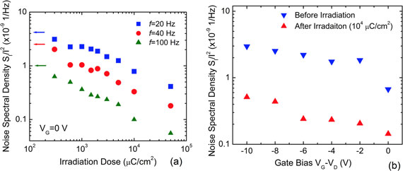 |
| Figure 3: Mechanism of the noise suppression in graphene. (a) The normalized noise spectral density, SI/I2, as a function of the radiation dose at zero gate bias for three frequencies f= 20, 40 and 100 Hz. The arrows indicate the level of 1/f noise before irradiation. (b) SI/I2 as the function of the gate bias (VG) referenced to the Dirac point (VD) for another graphene device before and after irradiation plotted for f=20 Hz. The negative bias corresponds to the hole-transport regime. Note that the noise suppression in graphene via defect engineering works in the entire range of biasing conditions and frequencies pertinent to practical applications. (The image is courtesy of Prof. Alexander A. Balandin) |
| “Although the reduction of 1/f noise after irradiation is unusual for conventional materials it is not unprecedented. There have been several reports when the 1/f noise decreased as a result of irradiation. However, in all previously reported cases of the 1/f noise reduction, a specific mechanism related to a particular device design was responsible for the observed effect. In our investigation, we employed the simplest device structure – generic graphene channel with a back-gate for controlling the number of carriers. It appears that the noise reduction phenomenon in graphene is of more general nature related to the characteristics of electron transport,” indicated Balandin. |
| The work at UCR was supported, in part, by the Semiconductor Research Corporation (SRC) and Defense Advanced Research Project Agency (DARPA) through STARnet Center for Function Accelerated nanoMaterial Engineering (FAME), and by the National Science Foundation (NSF) projects US EECS-1128304, EECS-1124733 and EECS-1102074. The work at RPI was supported by the US NSF under the auspices of I/UCRC “CONNECTION ONE” at RPI and by the NSF EAGER program. Dr. S. Rumyantsev was partially supported by the Russian Fund for Basic Research (RFBR) grant 11-02-00013. |
 By
Michael
Berger
– Michael is author of four books by the Royal Society of Chemistry:
Nano-Society: Pushing the Boundaries of Technology (2009),
Nanotechnology: The Future is Tiny (2016),
Nanoengineering: The Skills and Tools Making Technology Invisible (2019), and
Waste not! How Nanotechnologies Can Increase Efficiencies Throughout Society (2025)
Copyright ©
Nanowerk LLC
By
Michael
Berger
– Michael is author of four books by the Royal Society of Chemistry:
Nano-Society: Pushing the Boundaries of Technology (2009),
Nanotechnology: The Future is Tiny (2016),
Nanoengineering: The Skills and Tools Making Technology Invisible (2019), and
Waste not! How Nanotechnologies Can Increase Efficiencies Throughout Society (2025)
Copyright ©
Nanowerk LLC
|

Become a Spotlight guest author! Join our large and growing group of guest contributors. Have you just published a scientific paper or have other exciting developments to share with the nanotechnology community? Here is how to publish on nanowerk.com. |
