| Posted: Jun 08, 2011 |
New approach to strain engineering graphene circumvents current methods' limitations |
| (Nanowerk Spotlight) Unlike silicon, graphene lacks an electronic band gap – the gap being an energy range that cannot be occupied by electrons – and therefore has no switching capability; which is essential for electronics applications. Opening an energy gap in graphene's electron energy spectrum is therefore a critical prerequisite for instance for creating graphene transistors. |
| That's where strain engineering of graphene comes in. Researchers have discovered that local strain in a graphene sheet can alter its conducting properties. By varying the amount of local strain, transport gaps can be tailored (see for instance: "Strain engineering graphene's transport"). |
| Strain engineering is a general strategy already employed in today's semiconductor manufacturing. Currently, there are numerous known ways where one could impart controllable strains onto graphene membrane. They includes strain morphologies such as wrinkles in clean suspended graphene, graphene balloons on templated substrate and graphene strain superlattices on a lattice mismatched substrate. |
| In new work, reported in the May 26, 2011, issue of Physical Review B ("Gaps tunable by electrostatic gates in strained graphene"), researchers from IBM TJ Watson Research Center, Instituto de Ciencia de Materiales de Madrid and Radboud University of Nijmegen present a new and novel mechanism for gap opening in strained graphene via electrostatic gates and show that it can be important also in realistic situations. |
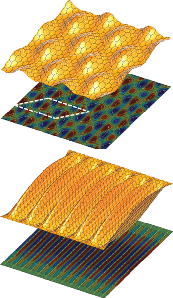 |
| Two strained graphene lattice configurations (upper panel) and their corresponding pseudomagnetic field (lower panel) studied in the paper, i.e., (a) strain superlattice and (b) wrinkled graphene. (Reprinted with permission from American Physical Society) |
| "We show that, when the pseudomagnetic fields created by long-wavelength deformations are appropriately coupled with an electric scalar potential, a significant gap can emerge due to the formation of a Haldane state – i.e. a quantum Hall insulator without application of magnetic field," Tony Low, a researcher with IBM's T. J. Watson Research Center, and the paper's first author, tells Nanowerk. "An example of a class of materials exhibiting the Haldane state is the topological insulator." |
| Low explains that, at present, all known ways of gap opening in graphene have a detrimental effect on the electron mobility: "In both biased bilayer and chemically functionalized graphene, one arrives at a disordered semiconductor with Mott variable range hopping mobility. In graphene nanoribbons, the mobility is typically several orders of magnitude smaller than bulk graphene. Our approach provides an attractive route to circumvent these limitations." |
| He points out that, of particular technological importance, he and his collaborators also consider setups where local or global gap can be tunable through simple electrostatic gates. |
| The research team, which also included Francisco Guinea from the Instituto de Ciencia de Materiales de Madrid and Mikhail I. Katsnelson from Radboud University of Nijmegen, envisions that their proposals can be applied to the various existing strategies for strain engineering graphene. |
| "If realized, this will open a new and, in our view, a very promising route to graphene-based electronics" says Low. |
 By
Michael
Berger
– Michael is author of four books by the Royal Society of Chemistry:
Nano-Society: Pushing the Boundaries of Technology (2009),
Nanotechnology: The Future is Tiny (2016),
Nanoengineering: The Skills and Tools Making Technology Invisible (2019), and
Waste not! How Nanotechnologies Can Increase Efficiencies Throughout Society (2025)
Copyright ©
Nanowerk LLC
By
Michael
Berger
– Michael is author of four books by the Royal Society of Chemistry:
Nano-Society: Pushing the Boundaries of Technology (2009),
Nanotechnology: The Future is Tiny (2016),
Nanoengineering: The Skills and Tools Making Technology Invisible (2019), and
Waste not! How Nanotechnologies Can Increase Efficiencies Throughout Society (2025)
Copyright ©
Nanowerk LLC
|

Become a Spotlight guest author! Join our large and growing group of guest contributors. Have you just published a scientific paper or have other exciting developments to share with the nanotechnology community? Here is how to publish on nanowerk.com. |
