Showing Spotlights 497 - 504 of 631 in category All (newest first):
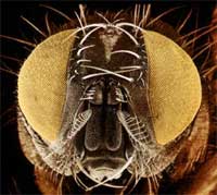 Looking at Nature as a successful design lab with millions of years of research experience, it is quite surprising that scientists haven't tried harder to copy some of Nature's more successful and impressive design blueprint. The list of actual commercialized biodesign-inspired products is very short. The most famous is Velcro, the hook-loop fastener that was invented in 1945 by Swiss engineer, George de Mestral. The idea came to him after he took a close look at the burrs (seeds) of burdock which kept sticking to his clothes and his dog's fur on their daily summer walks in the Alps. He examined their condition and saw the possibility of binding two materials reversibly in a simple fashion. And then, of course, there are the Wright Brothers, who modeled their planes on the structure of bird wings. Today, there are quite a number of terms such as bionics, biomimetics, biognosis, biomimicry, or even 'bionical creativity engineering' that refer to more or less the same thing: the application of methods and systems found in Nature to the study and design of engineering systems and modern technology. The use of design concepts adapted from Nature is a promising new route to the development of advanced materials and increasingly nanotechnology researchers find nanostructures a useful inspiration for overcoming their design and fabrication challenges. Because biological structures are the result of hundreds of thousands of years of evolution, their designs possess many unique merits that would be difficult to achieve by a complete artificial simulation. However, utilizing them as biotemplates and converting them to inorganic material could be a highly reproducible and low-cost process for fabricating complex nanostructures with unique functions. Complex functional systems are still out of reach but the replication of biological structures is making good progress. A recent example is the fabrication of antireflection nanostructures by replicating fly eyes.
Dec 19th, 2007
 Even the smartest scientists can still learn from the dumbest animals - at least as far as materials science is concerned. Take for instance marine glass sponges such as the hexactinellid sponge Euplectella sp. which are considered to be one of the most primitive animals in existence. Nevertheless, they produce integrated composite materials with outstanding mechanical properties and researchers are interested in finding out how they do that and how this natural process could be copied and adapted for use in the fabrication of synthetic composite materials. Euplectella's bioglass filaments, for instance, exhibit a rather complex design, thus ensuring the control of both mechanical and chemical interfaces between the different components to overcome the brittleness of the main constituent material, glass. Scientists have found that the amazing properties of many biological high-performance materials such as bone or shells are a result of the structure and the interplay of the constituents. In other words, the hierarchical structure of composites determines their material properties, and not the type of the composite's constituents. Researchers in Germany have now reported a biomimetic approach for the fast fabrication of hierarchically structured peptide-silica fibers, mimicking the bio-silicification process of natural glass fibers.
Dec 18th, 2007
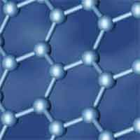 As a critical component of optoelectronic devices, transparent conductive coatings pervade modern technology. The most widely used standard coating is indium tin oxide (ITO), used in nearly all flat panel displays and microdisplays. Causing problems for manufacturers, though, Indium is expensive and scarce and demand is increasing. From the depressed levels of $60/kg in 2002, indium prices rose to over $1,000/kg during the summer of this year. Recently, prices have fallen back to between $400-$500/kg. But, geologists say the cost of indium may not matter soon, because the earth's supply of this element could be gone within just a few years. In addition to the limited availability of Indium there are other reasons that make ITO and other metal oxides such as FTO (fluorine tin oxide) increasingly problematic for electronics manufacturers: the instability of these metal oxides in the presence of acid or base; their susceptibility to ion diffusion into polymer layers; their limited transparency in the near-infrared region; and lastly, the current leakage of FTO devices caused by FTO structure defects. This has made the search for novel transparent electrode materials with good stability, high transparency and excellent conductivity a crucial goal for optoelectronic researchers. Recent work by researchers in Germany exploits ultra-thin transparent conductive graphene films as window electrodes in solar cells.
Dec 17th, 2007
 Past studies of photo-responsive proteins have generally dwelled on applications for energy-saving computer displays, light-based computing or computer memory. The general theme in the research tends to rely on the controllable and quick state change of the protein. But, the ability of the protein to actually incite a physical change in a composite macroscopic system has been largely unexplored. Harnessing this ability of the protein to incite change in a polymeric material could have broad implications in the field of biomedical and materials engineering. Getting bacteriorhodopsin to 'play ball' with other bulk materials could render those materials sensitive to a light. As a stimulus, light is often much easier to control than those typically explored by researchers such as bulk pH, temperature or electric fields.
Dec 13th, 2007
 The Bronze Age technique of soldering - a process in which two or more metal items are joined together by melting and flowing a filler metal into the joint - seems to be working just fine in the nanotechnology age. Researchers in California have developed an alternative method, effectively a miniaturization of soldering, to electron beam lithography (EBL) which, so far, is the method of choice for making electrical contact to nanostructures is. Carbon nanotubes, for instance, have been soldered together by using electron beam deposited gold molecules. There is a downside to using EBL as an industrial fabrication process: commercially used dedicated e-beam writing systems are very expensive (millions of dollars per unit), the process is complex, time-consuming and not really suitable for high-volume manufacturing, and there is a risk of sample contamination build-up on the samples. Other lithography-free contacting techniques such as shadow masks have been attempted, but they have their own drawbacks and have not been widely used. The new nano-soldering technique allows to make submicron sized, Ohmic contacts to nanostructures of even single atom thickness. The technique is simple, inexpensive, rapid, and entirely avoids sample contamination.
Dec 10th, 2007
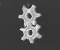 Machines usually require various components such as bearings, gears, couplings or pistons. As machines shrink to the micro- and ultimately nanoscale, their components of course need to shrink with them. One of the major obstacles to the realization of intricate nanomachines like nanorobots is the lack of effective processes for building freestanding nanocomponents with specific shapes and sizes. Self-assembly methods produce both organic and inorganic nano-objects with high yields through 'bottom-up' approaches. The shapes, however, in most cases are confined to rather simple forms such as spheres, rods, triangles and cubes etc. and are not suitable for the elementary components of intricate nanomachines. Meanwhile, the 'top-down' approaches including electron beam lithography and micro-contact printing etc. focus on surface patterning or fabrication of suspended objects, although they can fabricate sophisticated nanostructures. So far, the fabrication and assembly of nano-objects with specific shapes and sizes that can act as elementary components for movable nanoelectromechanical systems (NEMS) is only at the conceptual stage. New research results coming from South Korea now offer the first step toward the realization of sophisticated nanomachines, designed to perform specific tasks, with overall dimensions comparable to those of biological cells.
Dec 4th, 2007
 An important property of polyaniline (PANi), a polymer, is its electric conductivity. This makes it suitable for the manufacture of electrically conducting fibers. Consequently, PANi and other conductive polymers have been extensively studied for optical and electronic applications and many practical syntheses of one-dimensional (1D) nanostructured PANi have already been developed. However, preparation of water-soluble, conductive PANi nanowires with controllable morphologies and sizes, especially with good processibility, is still a big challenge. A possible solution could lie in the use of self-assembled proteins, such as plant viruses, as nanotemplates for the synthesis of these nanowires. For instance, genetically modified viruses have already been proposed as templates for the assembly of nanometer-scale components of electronic circuits. Researchers now have successfully demonstrated the fabrication of water-dispersible, conductive PANi nanowires using the rod-like tobacco mosaic virus (TMV) as a template. They have also shown that much longer conductive PANi/TMV nanowires (greater than the length of a native TMV particle) can be formed by a hierarchical assembly process.
Nov 30th, 2007
 In October, Sony introduced the world's first OLED (organic light-emitting diode) television set. This The 11-inch OLED TV - although quite expensive at $1,700 - realizes an astonishing 3mm-thinness (at thinnest point) and unparalleled image quality. What makes OLEDs so attractive is that they do not require a backlight to function and therefore they draw far less power and, when powered from a battery, can operate longer on the same charge. OLED devices can be made thinner and lighter than comparable LED devices. Another major leap forward compared to current display technologies is that OLEDs can be printed onto almost any substrate with inkjet printer technology, making new applications like displays embedded in clothes or roll-up displays possible. Unfortunately there are also drawbacks to this technology, in particular its currently high manufacturing cost. A possible solution could lie in cost efficient mass production methods using printing or spraying techniques. These methods use semiconductor materials that are processed in the form of a dispersion, comprising soluble conjugated polymers or precursor molecules as well as colloidal, organic or inorganic nanoparticles. Inkjet-printing represents a powerful, economic tool for accurate deposition of liquids which is not only useful for graphics applications, but has also enormous potential for the direct writing of electronic devices. Researchers in Austria have now shown for the first time the highly reproducible ink-jet printing of semiconducting nanocrystals for the fabrication of optoelectronic devices.
Nov 27th, 2007
 Subscribe to our Nanotechnology Spotlight feed