| Posted: May 31, 2010 | |
Bottom-up fabrication of carbon nanosystems by trapping single metal atoms |
|
| (Nanowerk Spotlight) Among the various production methods for carbon nanotubes (CNT) and graphene, currently only chemical vapor deposition techniques demonstrate a significant opportunity for mass production of CNT material. Using the CVD process, which is based on the catalytic action of metals, manufacturers can combine a metal catalyst such as iron with reaction gases such as hydrogen to form carbon nanotubes inside a high-temperature furnace. This process creates CNTs that are subsequently deposited in a collection environment and harvested into the desired end-product structural form. | |
| In order to optimize the synthesis process, a detailed understanding of the interaction between nanotubes or graphene and metal atoms is required – something that has been missing so far. Another area where specific knowledge of metal-carbon interfaces in electrical contacts is required is the fabrication of nanoelectronic devices. | |
| Researchers in France have now shown that it is possible to create atomic-scale defects in carbon nanotubes and in graphene in preselected positions with a focused electron beam and to use these defects as trapping centers for foreign atoms. By applying such a technique of subnanometer structuring, metal atoms can be placed in selected locations in graphene or nanotubes. | |
| Being able to replace single atoms in a graphenic network, this process promises an enormous potential in the development of new composite nanosystems with dedicated functions from the bottom up. | |
| "It has been known that the mobility of most foreign species on perfect graphene is too high for localizing these species" Florian Banhart tells Nanowerk. "Now we show that defective lattices can trap metal atoms. The motivation of our work has initially been the structuring of carbon materials with sub-nanometer precision. This was successful for pure nanotubes and graphene: stable vacancies could be created. However, while doing this on samples with metallic impurities, we saw that the vacancies were filled with metal atoms a short time after the vacancies have been created." | |
| Banhart, a professor at the Institut de Physique et Chimie des Matériaux (IPCMS) at the University of Strasbourg in France, and his group, have reported their method to trap metal atoms in graphene layers and carbon nanotubes in the May 25, 2010 online edition of ACS Nano ("Trapping of Metal Atoms in Vacancies of Carbon Nanotubes and Graphene"). | |
 |
|
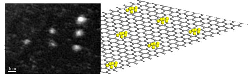
| Patterning of a graphene sheet by an automatic electron beam control. Mo atoms are trapped by the large vacancies created by focusing the electron beam on a triangular set of spots. (Image: Dr. Banhart, Université de Strasbourg) | |
| Normally there is no space for foreign atoms when the graphenic lattice is perfect because the carbon atoms are densely packed in the cylindrical or planar lattice. However, if carbon atoms are missing – i.e. when vacancies exist – there is space to trap other atoms but there are also open carbon bonds for attaching the other atoms. | |
| "We have created vacancies in nanotubes and graphene by focusing an extremely fine electron beam onto the objects and so knocking out carbon atoms," explains Banhart. "We observe that mobile metal atoms – that we have in the samples – are trapped in these vacancies and remain there. In such a way we can create a pre-defined pattern of metal atoms on nanotubes or graphene." | |
| This process is related to electron beam lithography, but here it works at an atomic scale. In effect, it allows the placement of metal atoms in selected locations in graphene or carbon nanotubes. | |
| "On the one hand" says Banhart, "we have shown that an Angstrom-size electron beam – in an aberration-corrected electron microscope – can be used for nanostructuring graphenic objects. On the other hand, we show a way how to attach metal atoms firmly to the graphenic lattice." | |
| The team's technique shows how graphene can be doped with metal atoms. For the application of graphene in electronic devices, doping seems necessary because graphene has a zero bandgap which is not ideally suited for switching. By attaching metal atoms, charge carriers can be injected into graphene and change the local density of states or shift the Fermi level. | |
| Banhart notes that, until now, graphene has been doped with species that were weakly attached on a perfect surface. "However, these species can easily diffuse on the surface or evaporate. Now, we have found a way of localizing dopants in specific positions." | |
| He also points out that a system of quantum dots can be made in such a way, leading to stationary electron waves in these patterned graphenic sheets and enabling the design devices with new functions. | |
| One of the challenges ahead for the team is the important task of carrying out electrical measurements on these metal-decorated graphene sheets or carbon nanotubes. These studies have to be carried out to study the influence of attached metal atoms on the electronic properties of graphenic devices. | |
 By
Michael
Berger
– Michael is author of three books by the Royal Society of Chemistry:
Nano-Society: Pushing the Boundaries of Technology,
Nanotechnology: The Future is Tiny, and
Nanoengineering: The Skills and Tools Making Technology Invisible
Copyright ©
Nanowerk LLC
By
Michael
Berger
– Michael is author of three books by the Royal Society of Chemistry:
Nano-Society: Pushing the Boundaries of Technology,
Nanotechnology: The Future is Tiny, and
Nanoengineering: The Skills and Tools Making Technology Invisible
Copyright ©
Nanowerk LLC
|
|
|
Become a Spotlight guest author! Join our large and growing group of guest contributors. Have you just published a scientific paper or have other exciting developments to share with the nanotechnology community? Here is how to publish on nanowerk.com. |
|