| Posted: Feb 14, 2006 | |
A new, low cost process to fabricate nanopillars |
|
| (Nanowerk News) A low cost nanosphere lithography method for patterning and generation of semiconductor nanostructures provides a potential alternative to conventional top-down fabrication techniques. A group of researchers at the University of Nebraska-Lincoln and the Lawrence Livermore National Laboratory reported their findings in an article "Fabrication of nanopillars by nanosphere lithography" in the Feb. 10, 2006 edition of the journal Nanotechnology. | |
| "This is a highly versatile, low cost strategy to fabricate nanometer and submicron scale pillar structures" Barry Cheung, one of the researchers, told Nanowerk. "We can apply it to silicon and III-Vs semiconductor substrates and many other materials. It is suited especially well for fabrication of self-aligned devices that can tolerate defective patterns." | |
| The researchers fabricated forests of silicon pillars of sub-500 nm diameter and with an aspect ratio up to 10 using a combination of the nanosphere lithography and deep reactive ion etching techniques. The nanosphere etch mask coated silicon substrates were etched using oxygen plasma and a time-multiplexed ‘Bosch’ process to produce nanopillars of different length, diameter and separation. Scanning electron microscopy data indicate that the silicon etch rates with the nanoscale etch masks decrease linearly with increasing aspect ratio of the resulting etch structures. | |
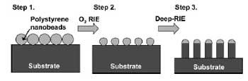 |
Schematic diagram of nanopillar fabrication by nanosphere lithography. Step 1: spin coat a hexagonally close packed monolayer of polystyrene beads on substrates. Step 2: tailor the size of the beads’ ‘resist’ by oxygen plasma etching. Step 3: etch the exposed semiconductor areas by deep reactive ion etching using the ‘Bosch’ process. (Source: University of Nebraska-Lincoln; Credit: Institute of Physics Publishing) |
| As an alternative to traditional nanosphere lithography methods, the researchers present a fabrication method that combines nanosphere lithography and reactive ion etching (both standard and deep) to produce hexagonally close packed semiconductor nanopillars. | |
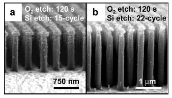 |
Scanning electron micrographs of nanopillars fabricated from a polystyrene bead patterned silicon surface pre-etched with a 120 seconds oxygen reactive ion etching period, followed by (a) 15 or (b) 22 cycles of the silicon etch process. (Source: University of Nebraska-Lincoln; Credit: Institute of Physics Publishing) |
| The researchers found that the etch process of their method is chemical transport rate limited. Since the patterns generated by nanosphere lithography depend on the geometry of the sphere packing, the reported scheme allowed only a single layer of patterned features to be generated on a substrate at a time. Also, the presented procedure yields only hexagonally close packed pillar patterns of limited domain size with diameters of tens of microns. | |
| However, applications which do not require perfect hexagonal patterns such as adhesion growth substrates for cell growth and the production of superhydrophobic surfaces can be envisaged with further chemical functionalization of the pillar surface. | |
| Unlike other gas phase nanowire synthesis, the new process does not require the patterning of a metal catalyst and thus minimizes the potential for unintentional doping of the wires. The challenge to generate a large domain size of packed nanospheres depends on the control of the phase of colloidal packing in the solution media and the interaction between the spheres and the substrates. Other research indicates, however, that there is a possible route to extend the limitation of the present procedure to generate nanopillar patterns with longer range order. Hence, the present demonstrated scheme provides an alternative inexpensive method for nanoscale, self-aligned pillar fabrication. | |
 By
Michael
Berger
– Michael is author of three books by the Royal Society of Chemistry:
Nano-Society: Pushing the Boundaries of Technology,
Nanotechnology: The Future is Tiny, and
Nanoengineering: The Skills and Tools Making Technology Invisible
Copyright ©
Nanowerk LLC
By
Michael
Berger
– Michael is author of three books by the Royal Society of Chemistry:
Nano-Society: Pushing the Boundaries of Technology,
Nanotechnology: The Future is Tiny, and
Nanoengineering: The Skills and Tools Making Technology Invisible
Copyright ©
Nanowerk LLC
|
|
Become a Spotlight guest author! Join our large and growing group of guest contributors. Have you just published a scientific paper or have other exciting developments to share with the nanotechnology community? Here is how to publish on nanowerk.com.