| Posted: Jun 02, 2014 | |
Spraying light - the fabrication of light-emitting 3D objects |
|
| (Nanowerk Spotlight) OLED (organic light-emitting diodes) technology is based on the phenomenon that certain organic materials emit light when fed by an electric current. What makes OLEDs so attractive is that they do not require a backlight to function and therefore require less power to operate; also, since they are thinner than comparable LEDs, they can be printed onto almost any substrate. The current commercial fabrication of OLEDs is a clean room technology that depends on time- and cost-driving process steps under high vacuum and/or inert atmosphere. This has limited OLED displays to smaller electronic devices such as phones, cameras and small TV screens. | |
| "The light-emitting electrochemical cell (LEC) shares several external attributes with the OLED, notably the opportunity for soft areal emission from thin-film devices, but its unique electrochemical operation eliminates the principal requirement on inert-atmosphere/vacuum processing as it can comprise solely air-stabile materials," Ludvig Edman, a professor at Umeå University in Sweden, who heads the Organic Photonics and Electronics Group there, tells Nanowerk. "This important intrinsic advantage has inspired recent work on an ambient-air fabrication of LEC devices using scalable means; but as-of-yet, a fault-tolerant and cost-effective fabrication of large-area and uniformly-emitting devices is lacking." | |
| Back in 2010, the group introduced A Unifying Model for the Operation of Light-Emitting Electrochemical Cells. Now, in cooperation with LunaLEC, a Swedish company that was formed in 2012 to commercialize the technology developed by Edman's group and Nathaniel Robinson's team at Linköping University, they have developed a spray-sintering method for the fabrication of LECs. | |
| "Spray-sintering is a new process of depositing material that works uniquely for LEC-fabrication," says Patric Stafshede, Managing Director of LunaLEC. "The common knowledge for fabrication of light-emitting devices has been that you need to deposit a wet, homogenous film of material in order to get a smooth surface without any pinholes in it that would create black spots or uneven emission. By contrast, the properties of the LEC allow for spraying layers that are inhomogeneous and that allows for spraying of individual droplets that dry one at a time." | |
| This has not been proven to work before and allows for moving some of the LEC-work from lab out in commercialization. | |
| Introducing a new, purpose-designed spray-sintering deposition technique, Edman's group now reports that it is possible to spray out liquid inks onto essentially any surface for the achievement of light emission. The findings have been published in the May 15, 2014 online edition of Advanced Materials ("Spraying Light: Ambient-Air Fabrication of Large-Area Emissive Devices on Complex-Shaped Surfaces"). | |
 |
|
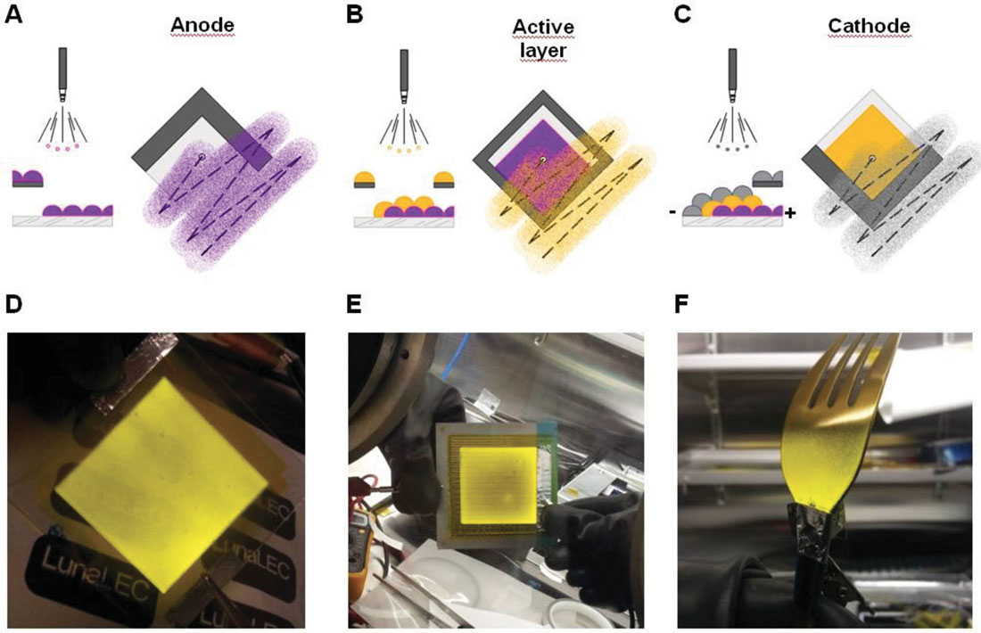
| Ambient spray-sintering of entire LEC structures, and the inclusion of light-emission function onto flat and complex-shaped metallic surfaces. (A-C) Schematic depicting the sequential spray-sintering of a bottom electrode, an active layer, and a top electrode. The shadow masks define the different layers for easy electrode contacting. (D) Light-emission from an all-spray-sintered LEC driven at V = 5 V. (E) Light-emission from an all-spray-sintered LEC, using an Al plate coated with a layer of PEDOT:PSS as the combined substrate and anode. (F) A light-emitting fork, as realized by spray-sintering a stainless-steel fork with an active layer and a top cathode. (Reprinted with permission from Wiley-VCH Verlag) (click image to enlarge) | |
| "Through sequential spraying of three thin layers of different inks onto the substrate-of-choice, we are able to realize uniform large-area light-emission at a low drive voltage of 3–5 V, and we are working toward the realization of any desired color" says Dr. Andreas Sandström, previously a researcher in Edman's group, now CTO of LunaLEC, and first author of the paper. | |
| He points out that the entire fabrication process can be executed under ambient air using a simple airbrush. | |
| The team also demonstrates that the inclusion of an additional sprayed layer allows for the creation of multi-colored light-emission patterns, and that light-emitting devices can be fabricated directly onto arbitrarily shaped surfaces. | |
| In case of the fork in the figure above (bottom-right image), the metal surface performed the dual function of substrate support and charge-injecting electrode, on top of which a multilayer LEC device structure was assembled via sequential spray-sintering. | |
| Stafshede explains that the motivation behind the work has been the potential to increase the size of the objects thr tram works with. "In the lab, we regularly have made 10mm by 10mm squares, but when we want to show the potential in the LEC-technology, homogenous light-emission over large areas, we need to fabricate larger area samples. The need for a reliable deposition technique over large areas – currently up to 20 cm by 30 cm – prompted this development." | |
| He notes that, initially, to develop the technology further, the technology will be used for marketing items, decorations or design applications where the unique form factors of the LEC are important. That means that to start with it will be used for 2D objects like small panels. | |
| "When spraying 3D-objects will become commercially viable, we will see both decorative and illumination applications," he adds. "A 3D-object can utilize already existing surfaces, for instance a door knob, for a child's night light, without the need to have additional light fixtures." | |
 By
Michael
Berger
– Michael is author of three books by the Royal Society of Chemistry:
Nano-Society: Pushing the Boundaries of Technology,
Nanotechnology: The Future is Tiny, and
Nanoengineering: The Skills and Tools Making Technology Invisible
Copyright ©
Nanowerk LLC
By
Michael
Berger
– Michael is author of three books by the Royal Society of Chemistry:
Nano-Society: Pushing the Boundaries of Technology,
Nanotechnology: The Future is Tiny, and
Nanoengineering: The Skills and Tools Making Technology Invisible
Copyright ©
Nanowerk LLC
|
|
|
Become a Spotlight guest author! Join our large and growing group of guest contributors. Have you just published a scientific paper or have other exciting developments to share with the nanotechnology community? Here is how to publish on nanowerk.com. |
|