| Posted: Oct 27, 2014 | |
Direct chemical contrast in STM imaging becomes available with new technique |
|
| (Nanowerk Spotlight) Scientists have developed a broad array of x-ray techniques for characterizing the surface morphology of materials. X-rays are very useful to investigate the structural, chemical, magnetic, and electronic properties of materials but the spatial resolution is very limited and these techniques cannot provide atomic resolution. | |
| A scanning tunneling microscope (STM), on the other hand, can be used to explore the atomic landscapes of the material surface. STM is not only useful for imaging material surfaces at the atomic scale, but also useful for determining the electronic, magnetic, and vibrational properties of materials at the atomic limit. Moreover, using atomic manipulations with STM, individual atoms can be positioned on a surface and quantum structures can be built on an atom-by-atom basis with sub-atomic precision. However, STMs are chemically 'blind'. | |
| Researchers have now demonstrated a technique that is a marriage between these two powerful methods and it promises simultaneous spatial and elemental information of the samples down to the atomic scale. By combining STM with synchrotron X-ray microscopy, there is now an instrument (SX-STM) that has the potential to perform all the applications of STM and X-rays in a single setting at the ultimate atomic limit. | |
| This achievement, published in the October 2, 2014 online edition of Nano Letters ("Elemental Fingerprinting of Materials with Sensitivity at the Atomic Limit"), is a result of scientific collaboration between Dr. Volker Rose’s and Prof. Saw-Wai Hla's research groups comprising of scientists from Argonne National Lab (Advanced Photon Source, Center for Nanoscale Materials, and Electron Microscopy Center) and researchers from Ohio University. | |
 |
|
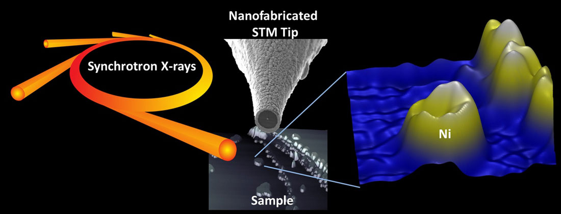
| In synchrotron X-ray scanning tunneling microscopy (SX-STM), synchrotron X-rays illuminate the sample. The resultant photo-electrons are tunneling into a specialized nanofabricated tip. The zoom in image at right shows a chemical image of 2 atomic layer thick Ni nanoclusters acquired at X-ray energy of 8.55 keV. (Image: Saw-Wai Hla and Volker Rose) (click on image to enlarge) | |
| Hla explains the working principle of this novel technique to Nanowerk: "Atoms have core level electrons, which are located at the orbitals closer to the atomic nucleus. Each chemical element in the periodic table has a specific set of core level electronic energies. One can excite the core level electrons with X-rays and use the excitation energy as a fingerprint to identify the types of elements. On the other hand, tunneling electrons used for STM imaging originate from the outer shell electrons near the Fermi level. So they do not have encoded elemental information. In synchrotron X-ray scanning tunneling microscopy (SX-STM), when the sweeping X-ray energy exceeds the energy of specific core level electrons, they are excited to produce photoelectrons. These photoelectrons then tunnel to the STM tip thereby producing a direct chemical element specific image with a very high spatial resolution." | |
| In this particular work, the researchers used nickel (Ni) nanoclusters adsorbed on a copper (Cu) crystal surface as the test samples. The smallest Ni cluster during this experiment is one atomic layer thick, and a few nanometers wide. | |
| "We achieve a direct elemental specific image of Ni cluster down to 2 nm spatial resolution at the ultimate sensitivity of single atomic height (0.2 nm)," says Rose. "Moreover, we are able to measure the X-ray cross section of a single Ni nanocluster for the first time. Normally, X-ray cross section are only averaged over a large area of the sample." | |
| To date, the direct elemental and chemical resolution achievable by synchrotron X-ray techniques is above 5 nm. Because synchrotron X-rays is extensively used in a wide spectrum of research areas including materials science, physics, chemistry, biology as well as medical and engineering applications, this new work could hugely benefit a large scientific community. | |
| Although the team experimentally demonstrated the working principle, theoretical understanding of photo-excited tunneling and light-matter interactions in SX-STM operation is still an open question to address. | |
| "Our measurements indicate that atomic resolution is achievable at low temperatures, and we are currently developing a new instrument that can operate at low temperatures down to 5 K (∼ negative 450 F)," notes Hla. "If it is completed, this will be the first low temperature instrument of such kind in the world." | |
| Potential application areas for synchrotron X-ray scanning tunneling microscopy could be to determine locations of specific metal atoms in brain samples; to identify elemental compositions in high capacity batteries; or to map magnetic domains at the atomic scale in new generation computer memory devices. | |
| Rose and Hla note that, in addition to the demonstration of atomic scale spatial resolution in elemental specific imaging, further research directions include testing its capability for chemical imaging such as oxidation states of the organic materials, and magnetic imaging such as elemental specific spin-polarized measurements of materials. | |
| "Eventually, we want to extend some biological specimen like brain tissues to map out its chemical compositions at the atomic scale," he says. | |
 By
Michael
Berger
– Michael is author of three books by the Royal Society of Chemistry:
Nano-Society: Pushing the Boundaries of Technology,
Nanotechnology: The Future is Tiny, and
Nanoengineering: The Skills and Tools Making Technology Invisible
Copyright ©
Nanowerk LLC
By
Michael
Berger
– Michael is author of three books by the Royal Society of Chemistry:
Nano-Society: Pushing the Boundaries of Technology,
Nanotechnology: The Future is Tiny, and
Nanoengineering: The Skills and Tools Making Technology Invisible
Copyright ©
Nanowerk LLC
|
|
|
Become a Spotlight guest author! Join our large and growing group of guest contributors. Have you just published a scientific paper or have other exciting developments to share with the nanotechnology community? Here is how to publish on nanowerk.com. |
|