| Posted: Feb 01, 2016 | |
'Multiplex number' as a new figure-of-merit for non-volatile resistive memory devices |
|
| (Nanowerk Spotlight) Resistive random access memory (RRAM) is envisioned as a next generation non-volatile memory because of the simple device geometry, ease of fabrication and operation. The necessity of high-density information storage and its relevance in neuromorphic circuitry has gained much attention and led to the development of multilevel resistive switching (MRS) for multiple memory states. | |
| In a recent study, researchers at the Jawaharlal Nehru Centre for Advanced Scientific Research (JNCASR), Bangalore, India, have defined a new figure-of-merit to identify the efficiency of resistive switching devices with multiple memory states. The research was carried out in collaboration with the Indian Institute of Technology Madras (IITM), Chennai, and financially supported by Department of Science and Technology, New Delhi. | |
| The results have been published in the January 8, 2016 online edition of Advanced Electronic Materials ("Defining Switching Efficiency of Multilevel Resistive Memory with PdO as an Example"). | |
 |
|
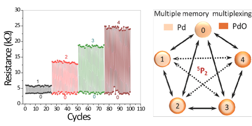
| By applying voltage pulses of different amplitude, electrical resistance is switched to multiple values. For a fabricated device, its ability to switch between any states is defined in terms of ‘multiplex number’. | |
| The scientists identified the versatility of palladium oxide (PdO) as a novel resistive switching material for use in resistive memory devices. Due to the availability to switch multiple redox states in the PdO system, researchers have controlled it by applying different amplitudes of voltage pulses. | |
| To date, many materials have shown multiple memory states but there have been no efforts to define the ability of the fabricated device to switch between all possible memory states. | |
| In this present report, the authors have defined the efficacy in a term coined as “multiplex number (M)” to quantify the performance of a multiple memory switching device: | |
 |
|
| Here n is the number of states, and γ is the number of fully possible switching events in between the memory states, and nP2 is the number of possible combinations of switching events in between the memory states. The first term enunciates the number of memory states in a device and the second term quantifies the fraction of switching events fully possible against the total number. Ideally, the second term should be unity. | |
| For the PdO MRS device with five memory states, the multiplex number is found to be 5.7, which translates to 70% efficiency in switching. This is the highest value of M observed in any multiple memory device. | |
| As multilevel resistive switching devices are expected to have great significance in futuristic brain-like memory devices, the definition of their efficiency will provide a boost to the field. The number M will assist researches as well as technologist in classifying and deciding the true merit of their memory devices. | |
|
By Dr. Abhay Sagade, Dept. of Engineering, University of Cambridge
|
|
|
Become a Spotlight guest author! Join our large and growing group of guest contributors. Have you just published a scientific paper or have other exciting developments to share with the nanotechnology community? Here is how to publish on nanowerk.com. |
|