| Posted: Jun 20, 2006 | |
The challenge of synthesizing magnetic nanostructures |
|
| (Nanowerk Spotlight) The scientific interest in magnetic nanostructures, both from a fundamental viewpoint and also due to their potential in a wide range of applications, over the past few years has led researchers to develop various nanofabrication methods for synthesizing nanomagnets. Applications for nanomagnetic materials include non-volatile magnetic random access memory MRAM, highly sensitive magnetic field sensor, field programmable spin logic, and patterned media for ultra high density data storage. | |
| A major challenge for technological applications of magnetic nanostructure arrays is the precise control of the magnetic switching processes. A good understanding of the magnetization reversal process is therefore needed in order to design tailor made novel magnetic devices. | |
| Researchers at the Information Storage Materials Laboratory (ISML) at National University of Singapore are conducting leading-edge scientific and engineering work in the field of magnetic nanostructures, spintronics and nanofabrication techniques. | |
| Professor Adekunle Adeyeye, a member of the ISML and a professor in the Department of Electrical and Computer Engineering, explains his group's recent work on nanofabrication methods for synthesizing nanomagnets to Nanowerk: | |
| "Our method uses deep ultra violet (DUV) lithography with aggressive resolution enhancement techniques followed by lift off. One unique advantage of this technique is the fact that unlike e-beam lithography, thicker resists can be used to make high aspect ratio nanostructures over a very large area. The technique is also compatible with the current semiconductor processing thus making the integration of magnetic devices on semiconductor platform achievable." | |
| The problem with some of the prevailing fabrication techniques, such as electron beam lithography (EBL), focused ion beam etching, x-ray lithography, nanoimprint lithography, and nanotemplating methods such as copolymer nanolithography, is that they have various limitations. | |
| "For example" says Navab Singh from the Institute of Microelectronics and a co-author of Adeyeye, "with EBL it is very difficult to fabricate closely packed high aspect ratio nanomagnetic arrays due to proximity effects. In addition, the writing process in EBL in most cases is serial and inherently slow, thus making large area fabrication extremely difficult." With some of the techniques magnetic nanostructures can only be fabricated over a relatively small area, thus limiting the type of magnetic characterizations that can be performed. | |
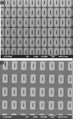 |
Two of Adeyeye's recent papers deal with nanoscale antidot structures, which have been proposed as a potential candidate for high density data storage. In the most recent paper, "Magnetic and transport properties of multilayer nanoscale antidot arrays", published in the May 29, 2006 edition of Applied Physics Letters, Adeyeye and his colleagues observed that by introducing nanoscale controlled pinning centers into an otherwise homogeneous multilayer film, giant magnetoresistance effects (GMR) can be realized. In another paper, "Magnetostatic interactions in mesoscopic Ni80Fe20 ring arrays", they demon- strated that the maximum achievable storage density of MRAM utilizing ferromagnetic rings is limited by the inter-ring spacing. The current efforts by Adeyeye and his collaborators are focused on developing new nanofabrication techniques for achieving sub-50nm large area nanomagnetic arrays. |
| Scanning electron micrographs of arrays of 20 nm thick Ni80Fe20 rings with different ring edge-to-edge spacing (a) s=100 nm (b) s=500 nm. (Reprinted with permission from the American Institute of Physics) | |
 By
Michael
Berger
– Michael is author of three books by the Royal Society of Chemistry:
Nano-Society: Pushing the Boundaries of Technology,
Nanotechnology: The Future is Tiny, and
Nanoengineering: The Skills and Tools Making Technology Invisible
Copyright ©
Nanowerk LLC
By
Michael
Berger
– Michael is author of three books by the Royal Society of Chemistry:
Nano-Society: Pushing the Boundaries of Technology,
Nanotechnology: The Future is Tiny, and
Nanoengineering: The Skills and Tools Making Technology Invisible
Copyright ©
Nanowerk LLC
|
|
Become a Spotlight guest author! Join our large and growing group of guest contributors. Have you just published a scientific paper or have other exciting developments to share with the nanotechnology community? Here is how to publish on nanowerk.com.