Nanotechnology News – Latest Headlines
Oscillating curves unhinge theories
Researchers have discovered previously unknown metallic features of high-temperature superconductors by running meticulously precise measurements.
November 9, 2009 Read more
Nanoelectric device detects liquids in luggage instantly
Restrictions on liquids in carry-on bags on commercial airliners could become a thing of the past thanks to a revolutionary nano-electric device which detects potentially hazardous liquids in luggage in a fraction of a second.
November 9, 2009 Read more
Joint School of Nanoscience and Nanoengineering Breaks Ground in Greensboro, NC
Unveiling plans for a 100,000(+)-square-foot research facility located at the South Campus of Gateway University Research Park in Greensboro, N.C., North Carolina Agricultural and Technical State University and The University of North Carolina at Greensboro will host the official groundbreaking of the Joint School of Nanoscience and Nanoengineering (JSNN) on Monday, Nov. 9.
November 8, 2009 Read more
More than 1,000 explore nanotechnology at UAlbany NanoCollege community day
The College of Nanoscale Science and Engineering of the University at Albany today welcomed more than 1,000 visitors of all ages from throughout upstate New York to participate in Community Day, part of CNSE's unprecedented community and educational outreach initiative known as NANOvember.
November 8, 2009 Read more
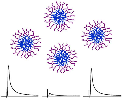
Promising nanomedicine approach for treating spinal cord injuries
Researchers at Purdue University have discovered a new approach for repairing damaged nerve fibers in spinal cord injuries using nano-spheres that could be injected into the blood shortly after an accident.
November 8, 2009 Read more
ChemMatters debuts first video podcast on nanotechnology's big impact
The American Chemical Society's award-winning high school chemistry magazine ChemMatters is making its YouTube debut with its first video podcast.
November 8, 2009 Read more
NanoTecNexus and NanoTumor Center launch first-of-its-kind webinar series
NanoTecNexus (NTN), formerly NanoBioNexus, already acclaimed for its educational forums and nanobiotechnology expertise, announces the launch of new courses, seminars, and lectures to be delivered online with proven and easy to use webinar tools.
November 8, 2009 Read more
Give your opinion on the Nanotechnology Research Code of Conduct
The European Commission has opened a public consultation in order to receive input from all people and organisations involved or interested in nanosciences and nanotechnologies research in Europe, and notably research, policy makers, industry, media and civil society organisations.
November 6, 2009 Read more
Presentations from the OECD Conference on the Potential Environmental Benefits of Nanotechnology
The speakers' presentations from the OECD 'Conference on Potential Environmental Benefits of Nanotechnology: Fostering Safe Innovation-Led Growth' are now available online on the OECD site.
November 6, 2009 Read more
Pre-announcement: Call for proposals within 'Energy Efficiency with Nanotechnology'
The Top-level Research Initiative is launching a call for user-driven research projects within the sub-programme 'Energy Efficiency with Nanotechnology' in the beginning of 2010.
November 6, 2009 Read more
New funding for development and deployment of UAlbany nanofabrication strategies
U.S. Senators Charles E. Schumer and Kirsten Gillibrand today announced that the Senate has approved the FY10 Commerce, Justice, Science, and Related Agencies Appropriations Bill which includes $500,000 for the University at Albany's College of Nanoscience and Engineering.
November 6, 2009 Read more
Advanced Researcher Grant 2009 an Nanowissenschaftlerin Luisa de Cola
Prof. Luisa De Cola vom Physikalischen Institut der Westfaelischen Wilhelms-Universitaet Muenster erhaelt eine besonders prestigetraechtige Auszeichnung des Europaeischen Forschungsrats (ERC): den hoch angesehenen 'Advanced Researcher Grant' 2009.
November 6, 2009 Read more
New synthetic molecules trigger immune response to HIV and prostate cancer
Researchers at Yale University have developed synthetic molecules capable of enhancing the body?s immune response to HIV and HIV-infected cells, as well as to prostate cancer cells.
November 6, 2009 Read more
Computer predicts reactions between molecules and surfaces, with 'chemical precision'
Good news for heterogeneous catalysis and the hydrogen economy: computers can now be used to make accurate predictions of the reactions of (hydrogen) molecules with surfaces.
November 6, 2009 Read more
Austria showcases its nanotechnology initiative
The 'NANO: Wissenschaft. Wirtschaft. Wirkung. 09' event the exhibition for the Austrian NANO Initiative of the BMVIT on 9 November at Tech Gate Vienna has been fully booked for a number of days.
November 6, 2009 Read more
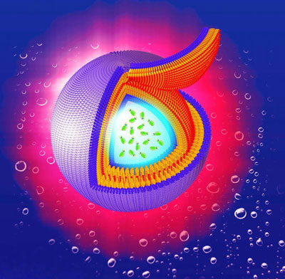
Nanocapsules for artificial photosynthesis
Chemists from the University of Wuerzburg have made progress on the road to achieving artificial photosynthesis.
November 6, 2009 Read more
 Subscribe to our Nanotechnology News feed