Nanotechnology Spotlight – Latest Articles
 Subscribe to our Nanotechnology Spotlight feed
Showing Spotlights 1937 - 1944 of 3577 in category All (newest first):
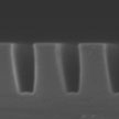
How nanostructure geometry affects polymer photovoltaic device efficiency
Conjugated polymer based organic photovoltaic (OPV) devices have been the subject of increasing research interest over the past years due to their potential of being light weight, mechanically flexible, semitransparent. To increase the efficiency of OPV, it is necessary to achieve a precisely controlled donor-acceptor phase separation within the short exciton diffusion length without dead ends, as well as a high hole mobility within the polymer. Now, researchers have demonstrated the effects of nanostructure geometry on the nanoimprint induced P3HT chain alignment and the performance of nanoimprinted photovoltaic devices.
July 22, 2014
DNA sequencing reaches new lengths
Sequencing technologies have made it cheaper and faster to read the sequence of bases on a strand of DNA. A promising technology to take these advances further is nanopore sequencing. Individual strands of DNA are moved through a nanopore gap not much wider than the DNA itself. As the DNA passes through the nanopore, continuous information is gained about the sequence of individual bases - the A, C, G and Ts that make up DNA. Researchers now have developed a nanopore sequencing technique reaching read lengths of several thousand bases.
July 17, 2014

Photorealistic plasmonic printing with aluminum nanostructures
Aluminum has gained interest in the field of nanoplasmonics not only because it is abundant and costs a fraction of gold or silver, but also because it allows field-enhancement effects into the ultraviolet. However, it has broader resonances than silver and gold, and forms an oxide layer. Both these effects are undesirable in applications such as biosensing, in which signal strengths are reduced in the presence of resistive losses and oxide barriers. However, color printing based on the plasmon resonances of aluminum nanostructures could benefit from these properties. Researchers have now demonstrated, for the first time, the utility of aluminum nanostructures for ultrahigh definition plasmonic color printing.
July 15, 2014
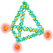
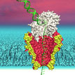
DNA nanopyramids detect and combat bacterial infection
One way to eliminate the toxicity issue of synthetic nanomaterials used in nanomedicine is by working with truly biocompatible natural carriers for sensing and drug delivery applications. The emerging field of DNA nanotechnology may provide a solution. In new work, researchers have developed a novel theranostic platform which is made by utilizing a self-assembled DNA nanopyramid as scaffold for incorporation of both detection and therapeutic moieties to combat bacterial infection.
July 11, 2014

Self-assembly machines - a vision for the future of manufacturing
Industrial production processes, by and large, rely on robotic assembly lines that place, package, and connect a variety of disparate components. While the manufacturing world is dominated by robots, there are applications where the established processes of serial 'pick and place' and manipulation of single objects reach scaling limits in terms of throughput, alignment precision, and the minimal component dimension they can handle effectively. By contrast, the emerging methods of engineered self-assembly are massively parallel and have the potential to overcome these scaling limitations.
July 10, 2014
Nanomaterial safety: An international collaboration on in vitro testing strategies
On September 15-16, 2014, come explore ways in which Alternative Testing Strategies (ATS) may be combined to create a Weight of Evidence (WOE) or 'multiple models' approach to inform context-specific decisions about risk from exposure to novel nanoscale materials. The goal is to advance a common understanding of the state of the science, early lessons, current opportunities, and next steps for developing ATS for use in decision making for nanoscale materials.
July 9, 2014
A universal and rapid method for transferring nanostructures
Many nanofabrication techniques depend on creating a structure on one substrate and then transferring it via various processes onto another, desired, substrate. Often, these methods are not generally applicable as they suffer from the process-specific drawbacks, such as for instance intolerance of transferred nanostructures to chemical etchant, and the harsh thermal environment needed. A novel universal and rapid method allows transferring nanostructures with various dimensions onto diverse substrates with high fidelity.
July 8, 2014
A room-temperature alternative to reducing the thermal conductivity of crystalline silicon
Thermoelectric materials hold great promise for turning waste heat back into useful power and are touted for use in hybrid cars, new and efficient refrigerators, and other cooling or heating applications. But they have one big drawback: they are very inefficient. Since thermoelectric devices work by maintaining a temperature difference between their different sides, it is important that the used materials have low conductivity, i.e. are good thermal insulators.
July 7, 2014