Nanotechnology Spotlight – Latest Articles
 Subscribe to our Nanotechnology Spotlight feed
Showing Spotlights 2545 - 2552 of 3575 in category All (newest first):

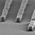
Nanotechnology on ice - novel lithography approach to nanodevice fabrication
Researchers at Harvard University have shown that nanostructures can be patterned with focused electron or ion beams in thin, stable, conformal films of water ice grown on silicon. They demonstrated ice lithography as a lithographic technique for patterning e.g. metal wires down to 20 nm wide. What's interesting about this technique is that patterning with ices of any condensed gas is a straightforward and practical process. Ice resist does not require spinning or baking. All processing and patterning steps can occur in a single evacuated chamber and be monitored at high resolution. The final removal of unexposed resist leaves minimal residues. Environmentally harmful solvents are not required and complete dry removal of the ice layer can be performed by in situ sublimation. Also, ice lithography makes it possible to nanopattern chemical modifications into silicon and other substrates. The team has now reported the successful application of ice lithography to the fabrication of nanoscale devices.
November 4, 2010

Nanotoxicology myth buster
Understanding the behavior and impacts of nanomaterials in the environment and in human health is a daunting task. Today, we don't even know what the impact of most chemicals is, and that includes products we have been using for many years. Nevertheless, a general understanding about nanotoxicity is slowly emerging as the body of research on cytotoxicity, genotoxicity, and ecotoxicity of nanomaterials grows. Many of the published toxicity studies have limited relevance, due, in large part, to study design limitations, including inadequate justification for dose selection or route of exposure criteria. A recently published article addresses myths and misconceptions regarding nanotoxicology.
November 2, 2010

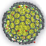
Buckyball polymers promise cheap, flexible solar cells
Compared to silicon-based devices, polymer solar cells made of conducting plastic material are lightweight, relatively inexpensive to fabricate, flexible, designable on the molecular level, and have little potential for negative environmental impact. The big question today is to what degree polymer solar cells will be able to commercially compete with silicon solar cells. With the exciting vision of organic solar cells becoming a low-cost electricity source available in any size and shape, as flexible thin films and even coatings, researchers all over the world are working on making organic solar cells commercially attractive. Finding a relatively simple way of polymerizing fullerenes and including this new material in photovoltaic cells, researchers have opened a route towards plastic solar cells that are much cheaper and easier to fabricate than conventional silicon-based photovoltaic panels.
November 1, 2010

Water desalination with graphene
A relatively new method of purifying brackish water is capacitive deionization (CDI) technology. The advantages of CDI are that it has no secondary pollution, is cost-effective and energy efficient. The basic concept of CDI, as well as electrosorption, is to force charged ions toward oppositely polarized electrodes through imposing a direct electric field: brackish water flows between pairs of high surface area carbon electrodes that are held at a potential difference of about 1-2 volts. The ions and other charged particles, such as microorganisms, are attracted to and held on the electrode of opposite charge. A research team has now developed a CDI application that uses graphene-like nanoflakes as electrodes for capacitive deionization. They found that the graphene electrodes resulted in a better CDI performance than the conventionally used activated carbon materials.
October 27, 2010

'Cooking' sharper AFM tips in a microwave oven
In atomic force microscopy (AFM), tip quality depends mainly on the dimensions and shape of the probe, the durability of the tip apex, and the nature of the interaction between sample and probe. With this in mind, researchers have experimented with mounting ultra sharp and high aspect ratio carbon nanotube (CNT) bundles onto the apex of an AFM tip to improve spatial and potential resolution. Although AFM tips functionalized with a carbon nanotube have attracted considerable attention, attaching CNTs to scanning probes is not a trivial matter, which limits their practical use. An alternative approach, whereby a CNT is grown onto the AFM tip, also can be very time-consuming and requires a costly set-up. A team at the Friedrich-Schiller-University Jena in Germany has now demonstrated a fast and cheap process for the fabrication of carbon nanotube AFM tips with the help of microwave ovens.
October 26, 2010

A nanomedicine approach for ocular neuroprotection in glaucoma
Medical researchers believe that the best way to protect eye from glaucoma is to protect the optic nerve from a sudden increase in intraocular pressure since ocular hypertension is the most important risk factor for glaucoma. Accordingly, for the past few years, huge research efforts have been made to develop a powerful biotechnical approach to protect the optic nerve. As a result, scientists discovered that Heat Shock Proteins (HSPs) can be a new powerful modality for the protection of optic nerves - ocular neuroprotection - from glaucoma. Although a variety of methods to induce HSPs have been developed and tried, they all were found to be ineffective for the induction of HSPs from the optic nerve due to side effects including chemical and physical side effects. A novel nanomedicine modality has now been shown to be feasible for ocular neuroprotection in glaucoma cases.
October 25, 2010
Novel nanopatterning technique uses liquid bridge to transfer materials from mould to substrate
Many nanotechnology research projects require some form of nanopatterning technique in fabricating the devices, structures and surfaces required. With the current state of micro- and nanofabrication, the direct printing of functional materials is the most efficient method at low cost and low environmental impact. A direct printing approach has the merits of forgoing complex and expensive equipment, reducing the fabrication processes, saving the amount of material used, and removing chemical exposure in the processes. However, imprinting methods suffer from residues and difficulty in multi-alignment. Researchers in Korea have now developed a direct printing technique that is based on a liquid-bridge-mediated transfer moulding process.
October 20, 2010
Nanodiamonds could revolutionize the current styrene synthesis industry
Catalytic dehydrogenation of ethylbenzene is one of the most important processes in the chemical industry world-wide. Styrene, for instance, is commonly produced using this process. The annual production of some 20 million metric tonnes of styrene is an important precursor in the plastics industry. Being able to develop a new metal-free, energy-saving, and efficient catalyst for alkane dehydrogenation would have a significant positive impact on the environment. Coke formation during the current industrial process is the main disadvantage of the metal-based catalysts now used. Steam is used as a protection agent to avoid coking and thus keep the catalysts active. The steam generation consumes massive amounts of energy. This is simply solved by using carbon as catalyst material. Even without steam, the catalyst is free from coke formation and shows long time stability. Researchers have now developed a new process for the dehydrogenation of ethylbenzene, using nanodiamonds as catalyst, that is oxygen-free and steam-free.
October 18, 2010