Nanotechnology Spotlight – Latest Articles
 Subscribe to our Nanotechnology Spotlight feed
Showing Spotlights 2553 - 2560 of 3575 in category All (newest first):

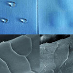
Electrofluidics device uses sub-10nm nanochannels to analyze DNA
In order to improve throughput speed of DNA sequencing and reduce its cost, researchers are pursuing real-time solid-state DNA sequencing devices. To that end, electronic functional devices in liquid environments need to be developed, ideally utilizing the compatibility with current complementary metal oxide semiconductor (CMOS) based fabrication technology. In this regard, the combination of electronics and nanofluidics leads to the field of electrofluidics, which utilizes the electrical behaviors of fluids for solid state device applications. In order to explore the ion transport and biomolecule transport through nanochannels, researchers have now reported the fabrication of an electrofluidic platform to study the motion of single molecules, including DNA. The device's nanochannel structures were fabricated with sub-lithographic dimension through top-down based, conventional semiconductor fabrication methods.
October 14, 2010
Nanotechnology improves wool fabrics
Nanotechnology shows great potential for revolutionizing the textile industry across its entire range of applications with its ability to impart new functionality to textiles while at the same time maintaining their look and feel. The wool textile industry, for example, is researching the development of textiles with fast-absorbing and quick-drying properties. This has great importance for improving clothing thermophysiological comfort and wearing performance by adjusting the transport of heat and moisture through a fabric which was usually achieved using synthetic fibers. One stubborn hurdle that prevents nanotechnology-enabled 'smart' textiles from becoming more of a commercial reality is the insufficient durability of nanocoatings on textile fibers or the stability of various properties endowed by nanoparticles. Quite simply put, the 'smart' comes off during washing. Developing an effective approach to enhance the coalesce force between nanoparticles and wool fibers has great significance both in scientific and real applications of nanotechnology functionalized textiles.
October 12, 2010
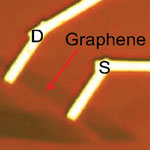
Novel graphene amplifier is a major step from single devices to circuits
So far, there have been no research reports on a graphene-based transistor amplifier and investigations of its in-field controllability for analog, mixed-signal, and radio-frequency applications. Previous work on graphene transistors has largely focused on frequency multiplication near the Dirac point in graphene current-voltage characteristic. But now, a team of researchers has demonstrated the first triple-mode graphene amplifier. They have shown experimentally that by leveraging the ambipolarity of charge transport in graphene, the amplifier can be configured in the common-source, common-drain, or frequency multiplication mode of operation by changing the gate bias. This is the first demonstration of a single-transistor amplifier that can be tuned between different modes of operation using a single three-terminal transistor. Moreover, during its operation, the graphene amplifier was configured in-field to switch between the different modes. The result marks another important step toward graphene applications in electronics.
October 11, 2010

Nanomechanical sensor can detect cholera
One of the tools developed by molecular biologists to study cell membranes and their associated proteins is a synthetic membrane model called Nanodisc. This is a self-assembled phospholipid bilayer disc of about 10 nm diameter, wrapped in a membrane scaffold protein belt. Nanodiscs render amphipathic and hydrophobic molecules easily soluble, offering transformative innovations across a broad range of applications in both in vivo delivery of therapeutics, diagnostic and imaging agents as well as for in vitro drug discovery. They have become important tools in analyzing membrane proteins, which are the most important target for present-day drug discovery programs. Further developing the nanodisc toolbox, researchers have now demonstrated the efficacy of Nanodiscs receptors for the nanomechanical detection of cholera.
October 7, 2010

Direct-growth fabrication for paper-based electronics
Zinc oxide is considered a workhorse of technological development exhibiting excellent electrical, optical, and chemical properties with a broad range of applications as semiconductors, in optical devices, piezoelectric devices, surface acoustic wave devices, sensors, transparent electrodes, solar cells, antibacterial activity etc. Thin films or nanoscale coating of ZnO nanoparticles are viewed with great interest for their many potential applications as substrates for functional coatings. Researchers in Taiwan have now shown, for the first time, that they can directly grow vertically aligned, highly crystalline and defect-free single-crystalline zinc oxide nanorods and nanoneedles on paper.
October 6, 2010
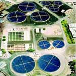
Researchers identify silver nanoparticles in sewage sludge of wastewater treatment plants
Silver nanoparticles are one of the most extensively used type of nanoparticles in consumer products due to the unique antibacterial activity of silver. There have been raising environmental concerns over their adverse ecological effects, along with ionic silver potentially released from the particles. To predict the environmental impact of engineered silver nanoparticles, their characterization from environmental matrices should be pursued, yet no field-scale studies are available to date. A new research report was motivated by the fact that silver nanoparticles in consumer products are likely being released during and/or after the product's lifetime. The silver nanoparticles will likely get into wastewater streams and subsequently enter wastewater treatment plants. During wastewater treatment processes, silver nanoparticles may be incorporated into the sewage sludge matrix and concentrated over time.
October 4, 2010
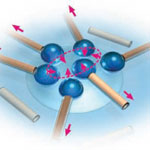
Walking on water
One of the (many) major challenges in getting closer to realizing visions of skillful nanomachines and ubiquitous nanofactories is the construction of synthetic nanomotors and other nanoscale propulsion systems that power these devices. At issue is not only the small scale of these systems but also the ability to precisely control their motion. Complicating the issue is that navigation principles used in the macroscale world are not applicable for nanoscale propulsion. The precise navigation of nanoscale objects is extremely challenging because of the combination of Brownian motion (random movement of particles) and low Reynolds number (where viscous forces dominate). Researchers in Germany have now demonstrated artificial water-walking devices in the form of self-powered microstriders at the air-liquid interface made of rolled-up catalytic microtubes.
September 30, 2010
The advantages of using functionalized fullerenes for cancer imaging and therapy
Gold-based nanostructures and carbon nanotubes have been successfully applied for photoacoustic imaging and photothermal treatment of tumors. Medical researchers believe that such nanoparticle-mediated, image-guided cancer therapy has tremendous promise for increasing the efficacy of cancer treatment while reducing toxic side effects traditionally associated with treatment. Working with a different carbon nanomaterial, researchers now have been able to show that polyhydroxy fullerenes can be utilized for the same purposes. The minute size and biocompatibility of polyhydroxy fullerenes make them particularly attractive for biomedical applications - they are water-soluble, biodegradable, antioxidant, and rapidly excreted.
September 29, 2010