Showing Spotlights 249 - 256 of 338 in category All (newest first):
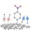 One item that so far has been missing from graphene's impressive list of physical properties is magnetism. In its pristine state, graphene exhibits no signs of the conventional magnetism usually associated with such materials as iron or nickel. So far, no reports that provide comprehensive evidence for either macro- or nanoscale magnetic phenomena for the ferromagnetism of carbon nanostructures in chemically functionalized graphene structures have appeared in the literature. Researchers have now filled this gap.
Nov 5th, 2013
 Material science is having a renewed influence on bioelectronics design beyond the incorporation of new functional nanomaterials. This newly established cooperation opens new windows for bioelectronics research, especially for fabricating flexible and smart devices. Recent advances in graphene research provide various possibilities to enhance performance characteristics and current approaches to design new bio-devices. Especially, smart and flexible bioelectronics on graphene has emerged as a new frontier in this area.
Oct 31st, 2013
 The future of your clothes will be electronic. Not only will electronic devices be embedded on textile substrates, but an electronics device or system could become the fabric itself. These electronic textiles will have the revolutionary ability to sense, compute, store, emit, and move - think biomedical monitoring functions or new man-machine interfaces, not to mention game controllers - while leveraging an existing low-cost textile manufacturing infrastructure. In new work, a group of scientists from Korea have now reported novel method for the fabrication of conductive, flexible, and durable graphene textiles wrapped with reduced graphene oxide.
Oct 29th, 2013
 Technology in our lives is ever more based on miniaturized structures that deliver higher performance devices taking up a fraction of the space compared to several years ago. But seeing what is going on at these tiny length scales comparable to molecules is very hard. Normally light cannot be used since it is not focused tightly enough, limited by the optical wavelength which is much larger than the structures we want to observe. New research suggests that tightly squeezing light into small gaps in metallic nanostructures now provides a way to circumvent this problem.
Oct 22nd, 2013
 Graphene-based nanomaterials have many promising applications in energy-related areas. In particular, there are four major energy-related areas where graphene will have an impact: solar cells, supercapacitors, lithium-ion batteries, and catalysis for fuel cells. Graphene could be a promising replacement material for indium tin oxide. A recent review provides an overview of research on graphene and its derivatives, with a particular focus on synthesis, properties, and applications in solar cells.
Oct 10th, 2013
 An increasing number of companies is involved in commercializing graphene on an industrial scale although the high cost of graphene is one of the major obstacles to its widespread adoption for commercial applications. The Nanomaterial Database we also list commercial graphene products and we keep a list of graphene manufacturers and suppliers that is constantly updated. Currently, this list contains 40 companies which are listed in this article.
Sep 19th, 2013
 In contrast to flexible electronics, which rely on bendable substrates, truly foldable electronics require a foldable substrate with a very stable conductor that can withstand folding, i.e. an edge in the substrate at the point of the fold, which develops creases, and the deformation remains even after unfolding. That means that, in addition to a foldable substrate like paper, the conductor that is deposited on this substrate also needs to be foldable. Researchers have now demonstrated a fabrication process for foldable graphene circuits based on paper substrates.
Aug 22nd, 2013
 Graphene has a unique combination of properties that is ideal for next-generation electronics, including mechanical flexibility, high electrical conductivity, and chemical stability. Combine this with inkjet printing, already extensively demonstrated with conductive metal nanoparticle ink, and you get an inexpensive and scalable path for exploiting these properties in real-world technologies. Although liquid-phase graphene dispersions have been demonstrated, researchers are still struggling with sophisticated inkjet printing technologies that allow efficient and reliable mass production of high-quality graphene patterns for practical applications. Recent work has addressed these issues and proposes an approach to overcome these problems.
Aug 20th, 2013
 Subscribe to our Nanotechnology Spotlight feed