Showing Spotlights 521 - 528 of 643 in category All (newest first):
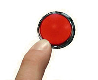
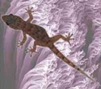 Animals that cling to walls and walk on ceilings owe this ability to micro- and nanoscale attachment elements. The highest adhesion forces are encountered in geckos. For centuries, the ability of geckos to climb any vertical surface or hang from ceilings with one toe has always generated considerable interest. A gecko is the heaviest animal that can 'stand' on a ceiling, with its feet over its head. This is why scientists are intensely researching the adhesive system of the tiny hairs on its feet. On the sole of a gecko's toes there are some one billion tiny adhesive hairs called setae (3-130 micrometers in length), splitting into even smaller spatulae (about 200 nanometers in both width and length) at the end. It was found that these elastic hairs induce strong van der Waals forces. This finding has prompted many researchers to use synthetic microarrays to mimic gecko feet. Recent work, mainly from A. Dhinojwala, P.M. Ajayan, M. Meyyappan, and L. Dai groups, as well as the Max Planck Institute for Metals Research in Germany (see our previous Spotlight: Gecko nanotechnology), has indicated that aligned carbon nanotubes (CNTs) sticking out of substrate surfaces showed strong nanometer-scale adhesion forces. Although carbon nanotubes are thousands of times thinner than a human hair, they can be stronger than steel, lighter than plastic, more conductive than copper for electricity and diamond for heat. Applications of such bio-inspired development of artificial dry adhesive systems with aligned carbon nanotubes could range from low-tech fridge magnets to holding together electronics or even airplane parts.
Nov 5th, 2007
 Nanotechnology enabled synthetic biology could one day lead to an artificial construct that operates like a living cell. That day might be a considerable distance off, given the difficulties scientists are still having in even understandiing the organizing principles and workings of a cell, not to mention being able to duplicate cell components and assembling them into a working whole. The large discrepancy between the functional density (i.e., the number of components or interconnection of components per unit volume) of cells and engineered systems highlights the inherent challenges posed by such a task. Just take 'simple' bacteria like Escherichia coli (which has an approx. 2 square micrometer cross-sectional area). The E. coli cell has some 4.6-million base-pair chromosome (the equivalent of a 9.2 megabit memory) that codes for as many as 4,300 different polypeptides under the inducible control of several hundred different promoters. The most advanced silicon chips will be able in a few years time to come close to this performance (on the other hand, you have several trillion E. coli in your gut; you would need to swallow a lot of computer chips to match this combined 'computing' power). Another way to look at the synthetic cell challenge is to regard the cellular environment as a highly complex synthetic medium, in which numerous multistep reactions take place simultaneously with an efficiency and specificity that scientists are not capable of duplicating at this scale. Researchers in The Netherlands have now succeeded in constructing nanoreactors that can be used to perform one-pot multistep reactions - another step towards the goal of artificial cell-like devices, but more promising in the short term for screening and diagnostic applications.
Oct 26th, 2007
 Proponents of 'atomically precise manufacturing' and 'molecular manufacturing' love to talk about the mind-boggling possibilities that these technologies would offer. These visions range from the modest, such as improved materials and more efficient production methods for chemicals (already on the horizon), to the outrageous, such as molecular desktop fabs (far, far out). Articles about revolutionary nanotechnology almost always skip the hard part, i.e. the tremendous amount of research breakthroughs that are required to get from where we are today to the promised land. It's as if some flight enthusiasts in 1903, when Orville Wright took off on the first powered flight, would have debated first class cabin design of 600-seat jet airliners flying New York - Tokyo non-stop. Nanotechnology researchers today are still struggling with very basic problems such as being able to control the synthesis of nanoparticles. It might come as a bit of a shock to the nanotechnology enthusiasts among you, but even something utterly fundamental as synthesizing metal nanoparticles today is more of an empirical trial and error approach than a predictable, fully controlled process. Let's take a look at new research coming out of a Spanish university that exemplifies the tiny, yet elementary, steps researchers need to take to master the nanoscale.
Oct 25th, 2007
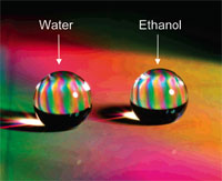 Contamination of superhydrophobic surfaces with low-surface-tension organic liquids is one of the leading reasons why superhydrophobic surfaces are not widely used in practical applications. If engineers were to succeed in creating a surface that repels any liquid the practical implications obviously would be substantial. In new work, researchers use metastable states to control wetting properties of solids. Since there is a much wider range of potentially available metastable states than thermodynamically stable states, the approach can greatly broaden the range of available control over the wetting behavior of solid surfaces.
Oct 23rd, 2007
 As Bubba in Forrest Gump pointed out, there are lots of possibilities with shrimps: "You can barbecue it, boil it, broil it, bake it ... there's ah... pineapple shrimp, lemon shrimp, pepper shrimp, shrimp soup, shrimp stew, shrimp salad, shrimp burger, shrimp sandwich...that's about it." It sounds pretty much the same when you listen to researchers talking about the numerous strategies for synthesizing nanoparticles - you can barbecue it, boil it, broil it, bake it (well, kind of) ... there's ah... sonochemical processing, cavitation processing, microemulsion processing, and high-energy ball milling. The problem is that, no matter what route you choose, nanoparticle synthesis is normally quite a tricky process that requires a lot of skill and expertise on the part of the chemist to obtain good quality particles of well controlled size and shape. Researchers in the UK tried to see if they could automate the whole procedure by preparing the nanoparticles in automated chemical reactors under the direct control of a computer. If successful, such reactors would find numerous applications in nanoscience and nanotechnology, especially in the areas of photonics, optoelectronics, bio-analysis and targeted drug delivery.
Oct 17th, 2007
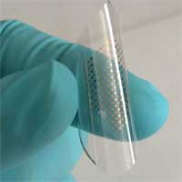 The problem with most current hydrogen sensor designs is that they are built on rigid substrates, which cannot be bent, and therefore, their applications might be limited due to the mechanical rigidity. In addition, they use expensive, pure palladium. A new type of sensors is bendy and use single-walled carbon nanotubes to improve efficiency and reduce cost. In the example of the space shuttle, laminating a dense array of flexible sensors on the whole surface of a pipe can detect any leakage of hydrogen prior to diffusion and alert control units to remedy the malfunction.
Oct 11th, 2007
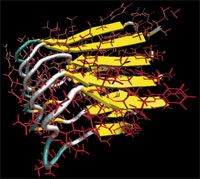 Nature is truly a brilliant nano engineer and has been so for billions of years. There is an abundance of 'smart' biological materials with hierarchical nanostructures - built from proteins - that are capable of adapting to new tasks, are self-healing, and can self-assemble autonomously simply out of a solution of building blocks. The performance and capability of these natural materials is something engineers can only dream of today. But by unlocking nature's secrets tiny step by tiny step, one day we will be able to not only duplicate but surpass the performance of natural materials. Only in recent years have scientists begun to understand the underlying principles and mechanisms of these materials - Why is spider silk stronger than steel? Why can cells be stretched reversibly several times of their original length? What kinds of molecular flaws lead to malfunctions in cells and tissues, as it occurs in Alzheimer's, rapid ageing disease progeria or muscle dystrophies, diseases in which the cell or tissue fails mechanically? Scientists at MIT have, for the first time, revealed the fundamental fracture and deformation mechanisms of biological protein materials, clarifying some long-standing issues about the deformation behavior of cells and Alzheimer's pathogens. The researchers report that the fracture mechanisms of two abundant nanoscopic building blocks of many proteins and protein materials exhibit two distinct fracture modes, depending on the speed of deformation. This is a surprising observation with far-reaching implications for the development of novel self-assembled protein materials and possibly the cure of certain genetic diseases
Oct 10th, 2007
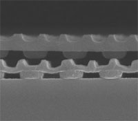 Nanoimprint lithography (NIL) has developed into a key technique for the fabrication of polymer nanopatterns and three-dimensional (3D) nanostructures. At its core, NIL is a simple nanometer scale pattern transfer process where a master mold with a desired pattern is used to fabricate identical patterns in an imprint resist, typically a polymer, with subsequent heat or light curing of the resulting mold. The attractivity of NIL comes from its capability for patterning with high resolution, high fidelity, high throughput, and low cost. Using NIL, nanometer sized patterns can easily be formed on various substrates, including silicon wafers, glass plates, flexible polymer films, and even nonplanar substrates. The limitation of conventional NIL techniques lies in their resulting patterned 2D layers; the formation of 3D micro- and nanostructures by stacking the 2D layers cannot be achieved by conventional NIL. That's why researchers came up with reverse nanoimprint lithography, a technique to transfer patterned 2D layers and to form multistacked 3D micro- and nanostructures on the substrate. While this works in principal, the achievable yields are very low due to the difficulty of detaching the master mold from the 3D structure. Researchers in South Korea have now managed to demonstrate the first successful fabrication of multi-stacked 2D nano patterned slabs on various substrates including flexible polymer film. This means real 3D nano structures such as photonic crystals can be fabricated with reasonable cost.
Oct 8th, 2007
 Subscribe to our Nanotechnology Spotlight feed