Showing Spotlights 545 - 552 of 643 in category All (newest first):
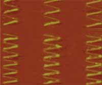
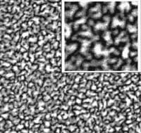 An incredible amount of research has gone, and still goes, into the understanding of the properties of nanoscale particles. In order to capitalize on that research, scientists and engineers have to take the next step, which is to turn nanoparticle laboratory results into usable materials and devices. One way to use engineered nanoparticles in the real world is in thin films. Nanoparticulate thin films are thin layers, sometimes only a few nanometers thick, of composite materials that contain nanoparticles. These new materials have a wide range of applications such as nanoelectronics, magnetic storage devices, or optical coating. However, most processes used to fabricate thin nanocomposite films with high nanoparticle fillings suffer from random nanoparticle agglomeration causing formation of irregularly shaped nanostructured features within the composite. Unfortunately, the improved mechanical, tribological and electrical properties of the nanocomposites over the host matrix materials (mostly polymers) are only attainable if the nanoparticle inclusions are of uniform size and shape with very good degree of dispersion. A newly developed technique now allows a wide range of control of including metal nanoparticle into polymer matrices in a single step process.
Jul 10th, 2007
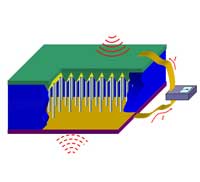 For the over 100 million people worldwide who suffer from diabetes, testing blood glucose is the only way to be sure that it is within normal range and allows them to adjust the insulin dose if it is not. The current method for monitoring blood glucose requires poking your finger to obtain a blood sample. The equipment needed to perform the blood test includes a needle device for drawing blood, a blood glucose meter, single-use test strips, and a log book. Now imagine this scenario: your doctor implants a tiny device the size of a rice grain under your skin. This device automatically and accurately measures your blood glucose levels at whatever intervals, even constantly if required. It transmits the data to an external transceiver. If any abnormality is detected, the device warns you and automatically transmits the data to your doctor's computer. This scenario is one of the many promises of nanomedicine where in-situ, real-time and implantable biosensing, biomedical monitoring and biodetection will become an everyday fact of normal healthcare. Nanosensors are already under intense development in laboratories around the world. One of the important components for implantable nanosensors is an independent power source, either a nanobattery or a nanogenerator that harvests energy from its environment, so that the sensor can operate autonomously. Not only has such a nanogenerator now been developed, but a new prototype has been demonstrated to effectively generate electricity inside biofluid, e.g. blood. This is an important step towards self-powered nanosystems.
Jul 6th, 2007
 Continuing miniaturization has moved the semiconductor industry into the nano realm with leading chip manufacturers well on their way to CPUs using 32nm process technology (expected by 2009). There are some real challenges ahead for chip designers, particularly in moving deeper and deeper into the nanoscale, where at some point in the near future they will reach physical limits of the traditional logic MOSFET (metal-oxide-semiconductor field-effect transistor) structure. In addition to physical barriers, semiconductor companies will also reach economic barriers where profitability will be squeezed hard in view of the exorbitant costs of building the necessary manufacturing capabilities if present day technologies are extrapolated. Quantum and coherence effects, high electric fields creating avalanche dielectric breakdowns, heat dissipation problems in closely packed structures and the relevance of single atom defects are all roadblocks along the current road of miniaturization. Enter nanoelectronics (note that microelectronics, even if the gate size of the transistor is below 100 nm, is not an implementation of nanoelectronics, as no new qualitative physical property related to reduction in size are being exploited). Its goal is to process, transmit and store information by taking advantage of properties of matter that are distinctly different from macroscopic properties. Understanding nanoscale transport and being able to model and simulate nanodevices requires an entirely new generation of simulation tools and techniques.
Jul 3rd, 2007
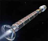 Nanotechnology will play an important role in future space missions. Nanosensors, dramatically improved high-performance materials, or highly efficient propulsion systems are but a few examples. In previous Nanowerk Spotlights we reported about nanotechnology propulsion technology, such as nano field emission thrusters, and the use of carbon nanotubes to harden electronic components in space. This last aspect, radiation shielding, is also where nanotechnology could make a major contribution to human space flight. NASA says that the risks of exposure to space radiation are the most significant factor limiting humans�?? ability to participate in long-duration space missions. A lot of research therefore focuses on developing countermeasures to protect astronauts from those risks. To meet the needs for radiation protection as well as other requirements such as low weight and structural stability, spacecraft designers are looking for materials that help them develop multifunctional spacecraft hulls. Advanced nanomaterials such as the newly developed, isotopically enriched boron nanotubes could pave the path to future spacecraft with nanosensor-integrated hulls that provide effective radiation shielding as well as energy storage.
Jun 29th, 2007
 Nanoimprinting lithography (NIL) is a simple pattern transfer process that is emerging as an alternative nanopatterning technology to traditional photolithography. NIL allows the fabrication of two-dimensional or three-dimensional structures with submicrometer resolution and the patterning and modification of functional materials. A key benefit of nanoimprint lithography is its sheer simplicity. There is no need for complex optics or high-energy radiation sources with a nanoimprint tool. There is no need for finely tailored photoresists designed for both resolution and sensitivity at a given wavelength. The simplified requirements of the technology allow low-cost, high-throughput production processes of various nanostructures with operational ease. NIL already has been applied in various fields such as biological nanodevices, nanophotonic devices, organic electronics, and the patterning of magnetic materials. Researchers at Berkeley have taken this process one step further by demonstrating that direct nanoimprinting of metal nanoparticles enables low temperature metal deposition as well as high-resolution patterning. This approach has substantial potential to take advantage of nanoimprinting for the application in ultralow cost, large area printed electronics.
Jun 27th, 2007
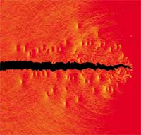 Bone is one of the most fascinating materials that has evolved in nature. There are 206 bones in your body - did you know that a newborn has 350 bones but they fuse together as you grow? - more than half of them in your hands and feet. These bones not only protect your organs, support your body against gravity's pull and allow you to move but they also are living tissues that produce blood cells and store important minerals. Not only important for humans, bones are the essential part of the endoskeleton of all vertebrates. Bone is a composite material of the mineral calcium hydroxyapatite and tropocollagen molecules (the fragile and soluble form of collagen when first synthesized by fibroblasts). It forms an extremely tough, yet lightweight material and its properties and behavior are of great interest to scientists and materials engineers. For instance, very little is known about the fracture behavior of bone and all such studies have been conducted at scales much larger than the nanoscale that explicitly considers individual tropocollagen molecules and mineral particles. New research at MIT has discovered a previously unknown toughening mechanism of bone that operates at the nanoscale - the level of individual collagen molecules and nano-platelets of hydroxyapatite. This breakthrough work lays the foundation for new materials design that includes the nanostructure as a specific 'design variable' and may help engineers to design materials from the bottom up by including hierarchies as a design parameter.
Jun 26th, 2007
 A lot of buzz has been created by the term "green nanotechnology". In a broad sense, this term includes a wide range of possible applications, from nanotechnology-enabled, environmentally friendly manufacturing processes that reduce waste products (ultimately leading to atomically precise molecular manufacturing with zero waste); the use of nanomaterials as catalysts for greater efficiency in current manufacturing processes by minimizing or eliminating the use of toxic materials (green chemistry principles); the use of nanomaterials and nanodevices to reduce pollution (e.g. water and air filters); and the use of nanomaterials for more efficient alternative energy production (e.g. solar and fuel cells). Unfortunately, there is a flip side to these benefits. As scientists experiment with the development of new chemical or physical methods to produce nanomaterials, the concern for a negative impact on the environment is also heightened: some of the chemical procedures involved in the synthesis of nanomaterials use toxic solvents, could potentially generate hazardous byproducts, and often involve high energy consumption (not to mention the unsolved issue of the potential toxicity of certain nanomaterials). This is leading to a growing awareness of the need to develop clean, nontoxic and environmentally friendly procedures for synthesis and assembly of nanoparticles. Scientists are now exploring the use of biological organisms to literally grow nanomaterials.
Jun 21st, 2007
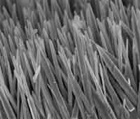 Large-scale and high-density semiconductor arrays with one-dimensional ("1D" - where one dimension of the structure is nanoscale) nanostructures have been extensively studied for their potential application in future electrooptical devices. Among them, zinc oxide (ZnO) is considered to be very attractive for high-efficiency short-wavelength optoelectronic nanodevices because of its large exciton binding energy of 60 meV and high mechanical and thermal stabilities. ZnO nanorod/ nanowire arrays have also been demonstrated to be highly versatile and proven to be quite effective in piezoelectric nanogenerators, dye-sensitized solar cells, photonic crystals, superhydrophobic surfaces, and even biodevices due to their biocompatibility. One of the issues researchers are still grappling with is the synthesis of ZnO nanowire arrays. On one hand, high-temperature techniques such as chemical vapor deposition (CVD) have been widely employed and result in high quality nanostructures. However, these methods are energy-consuming and expensive. On the other hand, there are several advantages of growing semiconducting nanostructures directly on conducting metal substrates, for instance the formation of robust electrical contacts during the growth. Such wet chemical methods, which are appealing for their low temperature, facile manipulation, and potential for scale-up have recently been developed for the production of aligned ZnO nanostructures and so far the most successful route has been seeded growth on ZnO-nanoparticle-coated substrates. In these two-step processes the coating of the substrate for the formation of a nucleation layer remains complex and difficult/irreproducible. Therefore, large-scale, low-cost controllable growth of well-aligned ZnO 1D nanostructures on properly fitting substrates via a one-step synthetic approach is still crucially needed for novel applications to become practicable. Researchers in China now have demonstrated exactly such a highly effective solution by growing well-aligned ZnO 1D nanostructures on various inert metal substrates at low temperature on a large scale.
Jun 18th, 2007
 Subscribe to our Nanotechnology Spotlight feed