Showing Spotlights 553 - 560 of 643 in category All (newest first):
 Thin, flexible displays have become an everyday component in many electronic gadgets from cell phones to digital cameras and MP3 players. Most of these displays are based on LCD technology, liquid crystals combined with polymeric structures, and one of their drawbacks is that their manufacturing cost grows rapidly with increasing screen size. A recently developed alternative approach for thin, flexible displays makes use of thermochromic composite thin-films. Thermo- chromism is the ability of a substance to change color due to a change in temperature. This first of a kind thermochromic display is based on films with thermochromic nanoparticles and embedded conductive wiring patterns. Based on the ease of fabrication and simple architecture, thermochromic displays could have advantages in lowering the display unit cost and, due to their heating pulse control scheme, can also lower power consumption compared with conventional displays.
Jun 14th, 2007
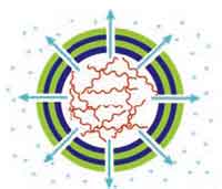 You cut yourself in the finger - and a few days later your skin has completely healed again. Biological organisms have an amazing ability to automatically initiate self-healing and self-repair when they sustain damage. Materials engineers are dreaming about making materials that could do the same thing. Imagine self-repairing cars, planes, bridges or buildings. These materials could be of particular use in structures that are at present impractical or impossible to repair, such as electronic circuit boards, implanted medical devices or spacecraft. Self-repairing materials would have a massive impact on virtually all industries, lengthening product lifetimes, increasing safety, and lowering product costs by reducing maintenance requirements. Thanks to nanotechnology, these visions are coming closer to reality. One approach is the use of nanocontainers that possess the ability to release encapsulated active materials in a controlled way, leading to a new family of self-repairing coatings.
Jun 13th, 2007
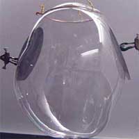 One of the most common methods of film manufacture is Blown Film Extrusion. The process, by which most commodity and specialized plastic films are made for the packaging industry, involves extrusion of a plastic through a circular die, followed by "bubble-like" expansion. The resulting thin tubular film can be used directly, or slit to form a flat film. Nanoscientists now have found a way to use this very common and efficient industrial technology to potentially solve the problem of fabricating large-area nanocomposite films. Currently, the problems with making thin film assemblies are either the production cost of using complex techniques like wet spinning or the unsatisfactory results of unevenly distributed and lumping nanoparticles within the film. The new bubble film technique results in well-aligned and controlled-density nanowire and carbon nanotubes (CNTs) films over large areas. These findings could finally open the door to affordable and reliable large-scale assembly of nanostructures.
May 31st, 2007
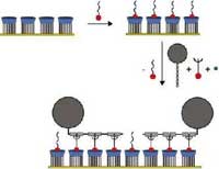 In 2005, researchers in the Netherlands developed the concept of a "molecular printboard" (named for its parallels with a computer motherboard) - a monolayer of host molecules on a solid substrate on which guest molecules can be attached with control over position, binding strength, and binding dynamics. Molecules can be positioned on the printboard using supramolecular contact printing and supramolecular dip-pen nanolithography. In this way, nanoscale patterns can be written and erased on the printboard. This technique, which combines top-down fabrication (lithography) with bottom-up methods (self-assembly), has now been applied to proteins. The resulting "protein printboards", allowing the capture and immobilization of proteins with precise control over specificity, strength and orientation, allows the fabrication of protein chips for applications in proteomics. They will play a major role in unraveling the human protein map, just as special chips were instrumental in mapping human DNA.
May 21st, 2007
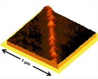
 Nanofluidic channels, confining and transporting tiny amounts of fluid, are the pipelines that make the cellular activities of organisms possible. For instance, nanoscale channels carry nutrients into cells and waste from cells. Researchers are trying to mimic Nature by constructing nanochannels in order to be able to manipulate single molecules in, predominantly biomedical, applications. Although nanochannels adjustable in size are prevalent in Nature, it is challenging to fabricate them artificially because of conflicting requirements for rigid structural integrity (to prevent collapse) on one hand and reconfigurability of nanometer-sized features on the other (to allow adjustability). Recent work at the University of Michigan addresses these issues and introduces methods to rapidly prototype structurally stable yet reconfigurable nanochannels. By fabricating tuneable elastomeric nanochannels for nanofluidic manipulation, the researchers were able to properly balance the need for flexibility and rigidity.
May 17th, 2007
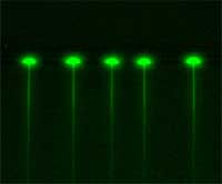
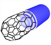 Current production methods for carbon nanotubes (CNT) result in units with different diameter, length, chirality and electronic properties, all packed together in bundles, and often blended with some amount of amorphous carbon. The separation of nanotubes according to desired properties remains a technical challenge. Especially single-walled carbon nanotube (SWCNT) sorting is a challenge because the composition and chemical properties of SWCNTs of different types are very similar, making conventional separation techniques inefficient. In order to find ways to control nanotube diameter and chirality it would be necessary to monitor nanotube growth. Then, if one knew exactly how to grow nanotubes of different characteristics, one could control their electronic properties because, depending on the way the carbon atoms are arrange around the 'waist' of a nanotube, the electronic properties could vary from metallic to semiconducting. An international group of researchers has demonstrated a novel approach to use nanotubes as reaction cells, enabling them to monitor the birth and growth of carbon nanotubes, and taking some spectacular image of this process.
May 10th, 2007
 Back in 1756, the German physicist Johann Gottlob Leidenfrost published a manuscript titled De Aquae Communis Nonnullis Qualitatibus Tractatus ("A Tract About Some Qualities of Common Water") in which he described a phenomenon in which a liquid, in near contact with a mass significantly hotter than its boiling point, produces an insulating vapor layer which keeps that liquid from boiling rapidly. This effect came to be called the "Leidenfrost Effect" and the associated temperature point the "Leidenfrost Temperature." An everyday example of this can be seen in your own kitchen: sprinkle a drop of water in a hot skillet - if the skillet's temperature is at or above the Leidenfrost Temperature, the water skitters across the metal and takes longer to evaporate than it would in a skillet that is hot, but at a temperature below the Leidenfrost point. Researchers in Germany have used this effect for a novel, template-free synthesis and patterning method of nanostructures.
May 9th, 2007
 One of the newly emerging areas of semiconductor technology is the field of transparent electronics. These thin-film materials hold the promise of a new class of flexible and transparent electronic components that would be more environmentally benign than current electronics. Being able to print transparent circuits on low-cost, flexible, plastic substrates opens up the possibility of a wide range of new applications, ranging from windshield displays and flexible solar cells to clear toys and artificial skins and even sensor implants. It is likely that such flexible see-through structures will find wide uses in military, biosensing and consumer goods due to the advantages of high transparency and reliable electrical characteristics. However, the emerging transparent electronics technology is facing manufacturing problems: current fabricating processes do not separate the device manufacturing from material synthesis. The transparent electronic materials, which are largely inorganic oxides. are directly deposited on the device substrate under harsh conditions which may cause damage to the existing layer or flexible substrate. The etching of small dimension oxide multilayer is also difficult due to the low selectivity of the etching recipe. New research results demonstrate that nanofabrication techniques could solve these problems.
Apr 30th, 2007
 Subscribe to our Nanotechnology Spotlight feed