Showing Spotlights 569 - 576 of 643 in category All (newest first):
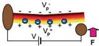 Piezoelectricity is a coupling between a material's mechanical and electrical behavior. When a piezoelectric material is squeezed, twisted, or bent, electric charges collect on its surfaces. Conversely, when a piezoelectric material is subjected to a voltage drop, it mechanically deforms. Many crystalline materials exhibit piezoelectric behavior and when such a crystal is mechanically deformed, the positive- and negative-charge centers are displaced with respect to each other. So while the overall crystal remains electrically neutral, the difference in charge center displacements results in an electric polarization within the crystal. Electric polarization resulting from mechanical deformation is perceived as piezoelectricity. This phenomenon was discovered by the brothers Pierre and Jacques Curie in 1880 and the word is derived from the Greek piezein, which means to squeeze or press. The piezoelectric effect finds useful applications such as the production and detection of sound, generation of high voltages, electronic frequency generation, microbalance, and ultra fine focusing of optical assemblies. For instance, types of piezoelectric motor include the well-known traveling-wave motor used for auto-focus in reflex cameras. A new research field, nanopiezotronics refers to generation of electrical energy at the nanometer scale via mechanical stress to the nanopiezotronic device. For example, bending of a zinc oxide nanowire transforms that mechanical energy into electrical energy. This new approach has the potential of converting biological mechanical energy, acoustic/ultrasonic vibration energy, and biofluid hydraulic energy into electricity, demonstrating a new pathway for self-powering of wireless nanodevices and nanosystems.
Mar 14th, 2007
 Since their discovery in the early 1990s, carbon nanotubes (CNTs) and carbon nanofibers (CNFs) have been used in a wide variety of applications. They have become indispensable in nanosciences and nanotechnology. However, because their production on an industrial scale remains expensive, their commercial use in such areas as catalysis has remained unthinkable. Current production processes including preparation of the support, normally silica or alumina, and impregnation with catalytically active metal for hydrocarbon decomposition, are not suitable for mass production. Researchers in Germany now report the fabrication of carbon nanotubes and carbon nanofibers on Mount Etna lavas used both as support and as catalyst, the first step for industrial production without preparation of support and its wet-chemical treatment. Such fabrication of CNTs/CNFs on naturally occurring minerals without synthetically prepared catalyst could pave the way for further exploitation of the superior properties of tailored nanostructured carbon for large-scale applications, such as catalysis and water purification by adsorption.
Mar 9th, 2007
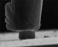 The earliest forgings, appearing around 1600 BC, were crudely hammered ornaments from naturally occurring free metals. The latest, most state-of-the-art forging techniques use micron-sized hammers to forge nanometer-sized metal shapes to be used as components in nanotechnology and microtechnology systems. New research demonstrates the possibilities of nanoforging - applying conventional metal shaping techniques to nano objects. In recent years, nanoscale fabrication has developed considerably, but the fabrication of free-standing nanosize components is still a great challenge. The ability to produce high-strength metallic components with characteristic dimensions of nanometers by nanoforging opens up new possibilities to eventually produce complex microsystems by assembling free-standing nanoscopic components. At these sizes they are of the same dimensions as micro-organisms and therefore sufficiently small even to travel through the human body.
Mar 7th, 2007
 Nanoelectronics devices often are made by integrating dissimilar classes of semiconductors and various other disparate materials into one heterogeneous single system. The two primary modes of combining these materials - mechanical bonding and epitaxial growth processes - place stringent requirements on the ultimate scale or constituent materials of circuits. With mechanical bonding, there is a limited ability to scale to large areas (i.e., larger than the wafers) or to more than a few stacking layers; incompatibility with unusual materials (such as nanostructured materials) and/or low-temperature materials and substrates; challenging fabrication and alignment for the through-wafer electrical interconnects; demanding requirements for planar bonding surfaces; and bowing and cracking that can occur from mechanical strains generated by differential thermal expansion and contraction of disparate materials. Epitaxy avoids some of these problems but places severe restrictions on the quality and type of materials that can be grown. Using a process akin to the printing press, researchers have managed to bypass the need for epitaxial growth or wafer bonding to integrate wide ranging classes of dissimilar semiconducting nanomaterials onto substrates for the purpose of constructing heterogeneous, three dimensional electronics.
Feb 27th, 2007
 While many dynamic systems are lubricated by fluids of various kinds, modern technologies, like aerospace, clean room equipment, medical devices and machines, require the application of dry coatings which exhibit reduced friction and wear. Lubrication of dynamic surfaces by fluids adds complexity, weight and cost to the system, which imposes various constraints and limits the performance of these systems. Self-lubricating coatings, i.e. coatings which exhibit reduced wear and friction without resorting to tribological fluids, have been known for many years and are in use for a variety of applications. Numerous studies have shown that different nanoparticles, impregnated into metal, polymer, ceramic and other coatings, can provide these materials with enhanced tribological performance. Prominent among these additives are the fullerene-like (IF) nanoparticles of tungsten disulfide (WS2) and molybdenum disulfide (MoS2). New research shows that it is possible to obtain self-lubrication of hard (i.e. dry) coatings such as cobalt by impregnating fullerene-like nanoparticles of WS2 in such coatings. The coating serves as a reservoir of nanoparticles which are slowly released from the surface and provide easy shear and reduced oxidation of the coating or native metal surface, which is a common phenomenon in tribology (friction and wear) of metallic surfaces.
Feb 21st, 2007
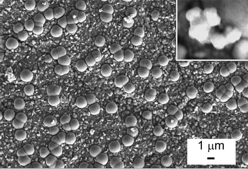
 Nanoparticles are of great scientific interest as they are effectively a bridge between bulk materials and atomic or molecular structures. Nanoparticles that consist of crystals of tens to thousands of atoms have been synthesized and used as "artificial atoms". In order to develop nanoparticle-based devices, though, it is essential to be able to control the placement of nanoparticles relative to one another. Two- and three-dimensional crystals of nanoparticles can be generated in a relatively straightforward manner, but it has been impossible to direct the assembly of the particles with any degree of specificity. The problem is that nanoparticle assembly so far has been constrained by the isotropic interactions between the particles. Isotropic materials have identical values of a property in all crystallographic directions, i.e. they are almost spherical in appearance. Though it is increasingly evident that nanoparticles would become a much more powerful research and engineering tool if it were possible to to enable directional assembly, breaking the interaction symmetry in isotropic materials is a major challenge. Doing so would enlarge the scope of potential applications, because anisotropic assemblies, where the interatomic bond strengths is directionally dependent, have distinctive properties that cannot be found or produced in isotropic assemblies. Researchers at MIT now have reported a simple method to fabricate divalent metal nanoparticles. This work is a first step towards enabling the controllable, directional assembly of nanoparticles into more complex and well-specified structures.
Feb 7th, 2007
 The combination of sp3, sp2, and sp hybridized atoms can give rise to a large number of carbon allotropic forms and phases, starting from carbon crystals based on all sp3 (diamond) and sp2 (graphite, fullerene) are well known and characterized. In addition there are innumerable transitional forms of carbon where sp2 and sp3 hybridization bonds coexist in the same solid such as in amorphous carbon, carbon black, soot, cokes, glassy carbon, etc. Solids based on sp hybridization, although subject of intense experimental efforts, seem to be the most elusive of the different carbon families. Such one-dimensional (1D) structures - "real" carbon nanowires - are linear chains of carbon atoms linked by alternating single and triple bonds (polyynes) or only double bonds (polycumulene). They are considered the building blocks for the elusive "carbyne": an ideal crystal constituted by carbon atoms with sp hybridization only. In solid and stable form this would represent a new carbon allotrope whose existence was a matter of great debate in the 1980s. With the immense interest in carbon nanomaterials, sp carbon nanostructures have become objects of renewed interest in recent years since they are considered precursors in the formation of fullerenes and carbon nanotubes; moreover they are interesting in astrophysics since they are considered constituents of interstellar dust. 1D carbon nanowires are expected to show interesting optical, electrical and mechanical properties. Some techniques already permit the synthesis of linear carbon chains in solution. However, their extremely high reactivity against oxygen - they can literally explode - and a strong tendency to interchain crosslinking makes synthesis of pure carbyne solids a major challenge. Researchers in Italy have now presented a simple method to obtain a solid system where polyynes in a silver nanoparticle assembly display long-term stability at ambient conditions.
Feb 5th, 2007
Micro-and/or nano-electromechanical systems (MEMS/NEMS) are the basis of future nanotechnology, because they combine miniature sensors and actuators with electronics. The selection of appropriate materials for MEMS/NEMS fabrication is based on the careful consideration of a material's properties with regard to its intended application. For example, many MEMS devices, such as pressure, chemical and bio sensors, rely on actuation of a membrane structure and require a high fracture toughness material for the enhanced durability and shock resistance. On the other hand, for fabrication of controlled nanostructures, the material should be machinable up to atomic level. Currently, the materials used for MEMS/NEMS fabrication are based on silicon or oxides, which are brittle and have size effects such as lattice defects, anisotropy, grains and grain boundaries. These effects are the limiting factors in the reduction of pattern size, especially when a dimension of the pattern approaches a few tenths of a nanometer. Researchers in Japan now have introduced zirconium-based glass thin films for the fabrication of 3D micro- and nanostructures. These materials exhibit excellent micro/nano-formability under very low stresses, and are expected to become one of the most useful materials for fabricating NEMS/MEMS devices.
Jan 26th, 2007
 Subscribe to our Nanotechnology Spotlight feed