Artificial Synapse: Definition, Materials, and Neuromorphic Applications
What is an Artificial Synapse?
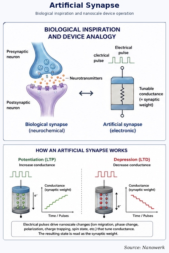
An artificial synapse is a nanoscale electronic or optoelectronic device whose state can be gradually adjusted by input signals, in a way that mimics the tunable, history-dependent connection strength of a biological synapse.
In simple terms, an artificial synapse is a tiny adjustable device that stores the strength of a connection in a neural-network-like circuit. In many devices this strength is represented by electrical conductance, so voltage or current pulses nudge the device into a slightly more conductive or less conductive state. In other designs, the weight may be represented by stored charge, polarization, magnetic configuration, ionic concentration, optical absorption, or another measurable device state.
An artificial synapse is not the same thing as an artificial neuron. The neuron generates, integrates, or processes signals; the synapse stores and adjusts the connection strength between neurons or circuit nodes. In neuromorphic hardware, many artificial synapses are arranged in arrays so that they can both store neural-network weights and help perform the multiply-accumulate operations that dominate machine-learning workloads.
This combination of storage and computation is central to neuromorphic engineering. Conventional CMOS computers usually move data back and forth between physically separate memory and processing units. Artificial synapse arrays reduce this data movement by keeping the weights where computation happens, which is why they are widely studied for energy-efficient AI accelerators and brain-inspired computing systems.
The motivation is scale and efficiency. The human brain is often estimated to contain about 1014 to 1015 synapses while operating at roughly 20 W. Estimates for the energy cost of a biological synaptic event vary, but they are commonly placed in the femtojoule range. Artificial synapse research tries to approach this combination of density, low energy, adaptability, and fault tolerance using nanoscale device physics.
The first widely cited demonstration of a nanoscale memristor acting as a synapse, including spike-timing-dependent plasticity, was reported in 2010. Since then, the field has expanded well beyond simple two-terminal memristors to include phase-change, ferroelectric, spintronic, electrochemical, organic, floating-gate, and photonic synapses.
Key takeaways:
- An artificial synapse stores the adjustable connection strength, or weight, between circuit nodes in neuromorphic hardware.
- Many artificial synapses encode this weight as conductance, but other physical states can also serve as the weight variable.
- Artificial synapses are different from artificial neurons: neurons process or generate signals, while synapses store and update connections.
- Common implementations include filamentary memristors, phase-change cells, ferroelectric devices, magnetic tunnel junctions, electrochemical transistors, floating-gate devices, and photonic synapses.
- The most important engineering distinction is between impressive single-device behavior and complete system performance, which also depends on arrays, interconnects, and CMOS peripheral circuits.
How an Artificial Synapse Works
A biological synapse adjusts its strength through processes that unfold on multiple timescales. Some changes are brief, such as paired-pulse facilitation lasting milliseconds to seconds. Others accumulate over repeated stimulation and can be described as long-term potentiation or long-term depression. Hardware synapses do not reproduce the full molecular complexity of biology; instead, they emulate selected mathematical features of synaptic plasticity that are useful for computation.
In a typical electrical artificial synapse, a presynaptic voltage pulse changes the device state by a small amount. A second terminal, gate, or output node reads the resulting state as a conductance, channel current, tunneling current, optical transmission, or other signal. Repeated pulses can accumulate into a larger change, and the state can either relax back with time for short-term memory or persist for longer-term weight storage.
The underlying physics differs strongly across device families. In oxide resistive memories, oxygen vacancies or metal ions move and reshape conductive paths. In phase-change memory, nanoscale regions switch between amorphous and crystalline phases. In ferroelectric devices, polarization domains are reoriented. In spintronic devices, magnetic order is rotated or moved. In electrochemical and organic transistors, ions enter or leave a channel. Each mechanism gives a different balance of speed, energy, retention, endurance, analog precision, and fabrication compatibility.
Synaptic plasticity in hardware
A useful artificial synapse usually needs to emulate selected plasticity rules inspired by biology. Paired-pulse facilitation means that the response to a second pulse is larger when it closely follows the first. This behavior can arise naturally from transient ionic motion, charge trapping, or thermal relaxation. Spike-timing-dependent plasticity (STDP) changes a weight depending on the relative timing of pre- and postsynaptic spikes, and it is one of the most common learning rules demonstrated in neuromorphic devices.
Hardware analogues of long-term potentiation and depression require gradual, repeatable state changes with retention long enough for the target application. For example, a synapse used for a temporary sensory filter may only need seconds or minutes of retention, while a synapse storing a trained neural-network weight may need months or years. Some diffusive memristors based on silver or other mobile ions provide an electronic analogue of short-term biological dynamics by switching between volatile and nonvolatile behavior depending on pulse strength and repetition rate.
Two-Terminal vs. Three-Terminal Artificial Synapses
Artificial synapses fall into two broad architectures. Two-terminal devices, including many resistive memory cells, phase-change materials, conductive-bridge cells, and some magnetic tunnel junctions, place the synaptic element between two electrodes. They integrate naturally into crossbar arrays, where one device sits at each row-column intersection. This layout enables very high density and direct analog matrix-vector multiplication, but the same path is often used for reading and writing, which can complicate programming and increase variability.
Three-terminal devices separate the write path from the read path, much like a transistor. A gate, electrolyte, floating gate, or programming electrode changes the channel state, while the source-drain path is read separately. This decoupling can improve linearity, update symmetry, and weight precision, which are important for on-chip training. The tradeoff is area: three-terminal synapses occupy more space and require more routing than the densest two-terminal crossbars. Recent organic field-effect transistor, electrochemical transistor, and ferroelectric transistor designs use this architecture.
Common Artificial Synapse Device Families
No single artificial synapse technology dominates. The main difference between device families is what physical state stores the synaptic weight. The right choice depends on whether the priority is density, speed, energy, analog precision, retention, endurance, biocompatibility, optical bandwidth, or compatibility with CMOS fabrication. The approximate energy ranges below refer mainly to reported device-level switching or programming events; full system energy can be much higher once drivers, interconnects, analog-to-digital converters, digital-to-analog converters, and control logic are included.
| Device family | Weight-storage mechanism | Approximate reported device-level energy | Strengths | Limitations |
|---|---|---|---|---|
| Filamentary RRAM (HfO2, Ta2O5, TiOx) | Formation, modulation, and rupture of oxygen-vacancy conductive filaments | Often pJ, with fJ-scale switching reported in optimized nanoscale devices | High density, fast switching, CMOS compatibility, sub-10 nm scaling potential | Cycle-to-cycle and device-to-device variability, nonlinear and asymmetric updates, sneak-path concerns in arrays |
| Conductive-bridge RAM (Ag/Cu in oxide or chalcogenide) | Migration of metal cations and formation of a metallic filament | Typically pJ to sub-pJ in demonstrations | Low programming voltage, high on/off ratio, natural short-term dynamics in diffusive modes | Filament stability, retention drift, stochastic switching |
| Phase-change memory (Ge2Sb2Te5 and related alloys) | Joule-heating-driven transitions between amorphous and crystalline phases | Commonly tens of pJ, with lower values possible in scaled cells | Multilevel storage, mature materials base, strong nonvolatility | Resistance drift, reset-current asymmetry, thermal crosstalk |
| Ferroelectric devices (HfZrOx, FeFET, FTJ) | Partial switching of polarization domains in ferroelectric layers | fJ to pJ reported, depending on geometry and readout | Fast operation, low-voltage options, two- and three-terminal designs | Endurance limits, depolarization fields, imprint, analog-state stability |
| Spintronic synapses (MTJ, domain-wall, skyrmion devices) | Magnetic configuration changed by spin-transfer torque or spin-orbit torque | Often pJ-scale in reported devices | Excellent endurance, nonvolatility, nanosecond switching | Limited analog levels per device, write-current demands, circuit complexity |
| ECRAM and organic electrochemical transistors | Reversible ion insertion, extraction, or gating of an electronic channel | fJ to pJ reported at small dimensions and low voltages | Highly linear and symmetric updates, good for on-chip training, soft and bioelectronic options | Slower programming, scaling challenges, electrolyte integration and retention tradeoffs |
| Floating-gate and charge-trap transistors | Charge stored on a floating gate or in trap states | Often fJ to pJ for read/write events, depending on programming method | Mature device concepts, long retention, precise analog tuning possible | Higher write voltages, slower programming, scaling constraints |
| Photonic and optoelectronic synapses | Optically driven carrier trapping, phase change, absorption change, or hybrid electronic-optical storage | Highly platform- and wavelength-dependent | High bandwidth, wavelength multiplexing, compatibility with optical neural networks | Larger footprint, optical-electrical conversion overhead, integration with electronic neurons |
A practical neuromorphic system is unlikely to be just a bare array of one device type. Most demonstrations combine synaptic devices with CMOS circuits for neurons, address decoders, pulse generators, sense amplifiers, digital-to-analog converters, analog-to-digital converters, and digital control. Some architectures also combine multiple synaptic devices or operating regimes so that short-term and long-term plasticity are handled separately.
How Nanoscale Engineering Enables Artificial Synapses
Most of the desirable properties of artificial synapses, including low energy, high density, and analog tunability, depend on nanoscale engineering. In a filamentary memristor, the active conductive path may be only a few nanometers in diameter, so switching involves rearranging a very small volume of material. In ferroelectric devices, nanoscale domains can provide multiple partially switched states. In spintronic devices, nanoscale magnetic textures or tunnel barriers define the weight state. In electrochemical devices, nanometer-scale ion transport paths determine speed, retention, and update linearity.
Research devices and arrays have demonstrated very small feature sizes, including crossbar pitches below 50 nm in some cases. However, high device density alone does not guarantee high system density or low system energy. Peripheral circuits, selector devices, isolation transistors, interconnect resistance, heat dissipation, and packaging all affect practical scaling. This is why artificial synapse development must combine materials engineering with array design and CMOS integration.
Materials and interfaces are tuned through atomic layer deposition, chemical vapor deposition, sputtering, etching, transfer printing, and solution processing. Controlled defect engineering sets where filaments nucleate or how ions move. Nanoionics describes the coupled ionic and electronic transport that underlies many resistive-switching and electrochemical synapses.
Two-dimensional materials, including graphene, transition-metal dichalcogenides, and h-BN, provide atomically thin 2D material channels, tunneling barriers, and defect-rich switching layers. Heterojunctions built from these materials can combine electronic, optical, and ionic responses in a single nanoscale device. Molecular, polymer, and biological materials are also being explored, especially for bioelectronics where compatibility with cells and tissues can matter more than maximum integration density.
Array-Level and System-Level Challenges
Single artificial synapses can show impressive switching energy, endurance, and analog behavior, but many problems only appear at the array level. Crossbar circuits must manage sneak currents through unselected devices, voltage drops along nanoscale wires, read noise, limited analog precision, thermal coupling, and parasitic capacitance. As arrays grow, line resistance and device variability can distort the matrix-vector multiplication that the array is supposed to perform.
Peripheral circuitry is another major bottleneck. Digital-to-analog converters are needed to apply input voltages, analog-to-digital converters are needed to read output currents, and pulse-generation circuits are needed for programming. These circuits can dominate area and energy, especially when the synaptic devices themselves switch at very low energy. For that reason, device-level claims such as femtojoule switching should not be confused with full-chip inference energy.
The most robust neuromorphic systems therefore use device-circuit-algorithm co-design. Algorithms can tolerate some device noise, quantization, and nonlinear updates; circuits can compensate for drift and variability; and materials engineering can improve the underlying synapse. Progress depends on optimizing all three levels together rather than treating the artificial synapse as an isolated memory cell.
Applications
In-memory computing accelerators
The largest near-term application is hardware acceleration of neural networks. Crossbar arrays of artificial synapses can perform multiply-accumulate operations directly in the analog domain: input voltages represent activations, device conductances represent weights, and summed output currents represent dot products. This approach is attractive because matrix-vector multiplication dominates many deep-learning workloads.
Research chips integrating thousands to millions of synaptic devices with CMOS peripherals have demonstrated image classification, speech recognition, and edge-learning tasks. These demonstrations show that analog in-memory computing can reduce data movement and improve energy efficiency for certain workloads. However, practical performance still depends strongly on device variability, calibration, ADC/DAC overhead, write endurance, and whether the system is used for inference only or for on-chip training.
Spiking neural networks and edge AI
Spiking neural networks process information through discrete events in time, making them a natural fit for devices that already respond to pulses and temporal history. Memristive, ferroelectric, spintronic, and electrochemical synapses can be paired with spiking-neuron circuits to build low-power classifiers, anomaly detectors, keyword spotters, and adaptive sensor interfaces.
Edge systems are a particularly important target because they often operate under tight power budgets and must process data locally. Artificial synapse arrays can sit close to sensors such as artificial retinas, tactile arrays, chemical sensors, or electronic skin. In such systems, the synaptic array can act as a learnable filter or feature extractor before data are transmitted elsewhere.
Bio-integrated and flexible neuromorphic systems
A more exploratory application area is bio-integrated neuromorphic hardware. Organic electrochemical synaptic transistors and other soft-material devices can operate at low voltages in ionic environments, which makes them attractive for adaptive interfaces with biological tissue. Possible long-term uses include closed-loop prosthetics, neural signal processing, and brain–machine interfaces, although these applications remain less mature than in-memory computing accelerators.
Combined with flexible and stretchable electronics, artificial synapses also support wearable sensory processing. A flexible synaptic array could be laminated on curved surfaces, robotic skins, or biomedical patches and perform local adaptation before wireless transmission. In these contexts, mechanical compliance, biocompatibility, and stable operation in humid or ionic environments may be more important than maximum switching speed.
Challenges and Future Perspectives
No artificial synapse technology, including its required peripheral circuitry, yet matches the brain's combination of density, efficiency, adaptability, and reliability. Device-to-device variability and cycle-to-cycle variability remain major sources of accuracy loss. Many devices also show nonlinear or asymmetric weight updates, meaning that potentiation and depression do not behave as mirror images. These imperfections complicate training and often require algorithmic compensation.
Endurance, retention, and analog precision are difficult to optimize simultaneously. A device optimized for long retention may switch slowly or require more energy. A device optimized for very low energy may suffer from drift or stochasticity. A device with excellent endurance may support too few stable analog levels. Retention requirements also vary widely: short-term plasticity may require milliseconds to seconds, while stored model weights may require months or years.
Three trends are shaping the next generation of artificial synapses. The first is heterogeneous integration, in which different device types or operating regimes are combined so each handles the timescale or precision it is best suited for. The second is three-dimensional and monolithic stacking, which aims to increase synaptic density using back-end-of-line nanofabrication compatible with conventional transistor technology. The third is co-design across devices, circuits, and learning algorithms, which treats analog imperfections as constraints to be managed rather than defects that must be completely eliminated.
As these trends converge, the role of the artificial synapse is expanding. It is no longer viewed only as a static memory cell that imitates a neural-network weight. Increasingly, it is treated as a dynamic computational element whose intrinsic time dependence, stochasticity, and material response can be used as part of the computation itself.
FAQ: Artificial Synapse
What is an artificial synapse in simple terms?
An artificial synapse is a tiny adjustable device that stores the strength of a connection in a neural-network-like circuit. In many implementations, electrical pulses gradually increase or decrease the device conductance, and that state remains after the pulse ends. Arrays of artificial synapses can therefore store neural-network weights and help perform computation in the same physical location.
How is an artificial synapse different from a memristor?
Most artificial synapses behave in a memristive sense because their present conductance or response depends on previous stimulation. However, not every artificial synapse is a two-terminal memristor, and not every memristor is a useful synapse. Synaptic devices can also be built from electrochemical, ferroelectric, floating-gate, photonic, or spintronic structures that store connection strength through mechanisms other than simple resistive switching.
Why do artificial synapses need to be nanoscale?
Nanoscale dimensions help artificial synapses reach high density and low switching energy. In filamentary resistive devices, for example, the active conduction path can be only a few nanometers wide, so only a small volume of material must be rearranged during programming. Nanoscale ferroelectric domains, ion channels, magnetic textures, and tunneling barriers similarly allow many synaptic states to be packed into compact hardware.
What are artificial synapses used for in practice?
The main near-term use is in-memory computing for neural-network acceleration, where crossbar arrays perform matrix-vector multiplication directly in hardware. Other targets include spiking neural networks for low-power edge devices, sensory processing in artificial retinas and electronic skin, adaptive robotics, and exploratory bio-integrated systems such as closed-loop prosthetics and brain–machine interfaces.
What are the main types of artificial synapse devices?
Major device families include filamentary resistive switches and conductive-bridge cells, phase-change memory cells, ferroelectric tunnel junctions and ferroelectric transistors, spintronic devices such as magnetic tunnel junctions, electrochemical random-access memory and organic electrochemical transistors, floating-gate or charge-trap transistors, and photonic or optoelectronic synapses.
How close are artificial synapses to the energy efficiency of the brain?
Individual artificial synapses can show very low device-level switching energy in research demonstrations, sometimes in the femtojoule to picojoule range. Full systems are less efficient because they also require peripheral CMOS circuits, drivers, interconnects, and analog-to-digital or digital-to-analog converters. Closing the gap with biological efficiency requires progress at the device, array, circuit, and algorithm levels.
Further Reading
Nature, Training and operation of an integrated neuromorphic network based on metal-oxide memristors
Nature Materials, Memristors with diffusive dynamics as synaptic emulators for neuromorphic computing
Nature Materials, A non-volatile organic electrochemical device as a low-voltage artificial synapse for neuromorphic computing
Nature Reviews Materials, Dynamical memristors for higher-complexity neuromorphic computing
