Nanostencil Lithography: A Versatile Nanopatterning Technique
What is Nanostencil Lithography?
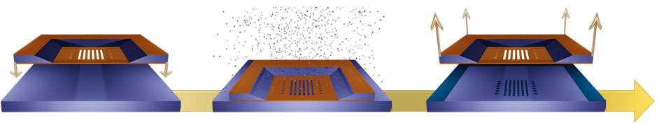
Nanostencil lithography (NSL) is a shadow-mask-based nanopatterning technique that allows for the direct deposition of materials through a stencil mask with nanoscale openings. It enables the fabrication of nanostructures and nanodevices without the need for resist-based processing or complex etching steps, making it a versatile and cost-effective method for nanoscale patterning.
Key Features of Nanostencil Lithography
Nanostencil lithography offers several distinct advantages over traditional nanolithography techniques:
- Simplicity: NSL is a single-step process that eliminates the need for complex resist-based processing, exposure, and development steps. It allows for the direct deposition of materials through a stencil mask, simplifying the nanopatterning workflow.
- Versatility: NSL is compatible with a wide range of materials, including metals, semiconductors, and organic compounds. It can be used to deposit nanostructures on various substrates, such as silicon, glass, and flexible materials, making it suitable for diverse applications.
- High resolution: NSL can achieve sub-100 nm feature sizes, depending on the stencil mask design and the deposition process. The resolution is primarily limited by the fabrication of the stencil mask, which can be optimized using advanced nanofabrication techniques.
- Parallel processing: NSL enables the simultaneous patterning of large areas through the use of stencil masks with multiple openings. This parallel processing capability allows for high-throughput fabrication of nanostructures and nanodevices.
Stencil Mask Fabrication
The fabrication of high-quality stencil masks is crucial for the success of nanostencil lithography. Stencil masks are typically made of thin silicon nitride (SiN) or silicon (Si) membranes with nanoscale openings. The fabrication process involves the following steps:
- Membrane preparation: A thin SiN or Si membrane is created using standard microfabrication techniques, such as low-pressure chemical vapor deposition (LPCVD) or silicon-on-insulator (SOI) wafer processing.
- Patterning: The desired nanoscale pattern is defined on the membrane using high-resolution lithography techniques, such as electron beam lithography (EBL) or focused ion beam milling. These techniques create openings in the membrane that will define the nanostructures on the substrate.
- Etching: The patterned membrane undergoes an etching process, such as reactive ion etching (RIE) or wet etching, to transfer the pattern through the membrane and create the stencil mask.
The fabrication of high-quality stencil masks requires precise control over the membrane thickness, pattern fidelity, and mechanical stability. Advanced nanofabrication techniques and materials, such as ultrathin membranes and robust support structures, are being developed to improve the performance and reliability of stencil masks.
Deposition Processes
Nanostencil lithography is compatible with various deposition processes, depending on the material and the desired nanostructure properties. Some common deposition processes used in NSL include:
- Physical vapor deposition (PVD): PVD techniques, such as thermal evaporation and sputtering, are widely used in NSL for the deposition of metallic and inorganic materials. These processes allow for the controlled deposition of thin films through the stencil mask openings.
- Chemical vapor deposition (CVD): CVD processes, such as plasma-enhanced CVD (PECVD) and atomic layer deposition (ALD), can be used in NSL for the deposition of conformal and high-quality thin films. These processes enable the deposition of materials with precise thickness control and excellent step coverage.
- Organic molecular beam deposition (OMBD): OMBD is a specialized deposition technique used in NSL for the deposition of organic materials, such as small molecules and polymers. It allows for the fabrication of organic nanostructures with well-defined morphologies and optoelectronic properties.
The choice of deposition process depends on the specific material requirements, such as purity, stoichiometry, and crystallinity, as well as the desired nanostructure properties, such as thickness, conformality, and aspect ratio.
Applications of Nanostencil Lithography
Nanostencil lithography finds applications in various fields, leveraging its ability to fabricate nanostructures and nanodevices with high resolution and versatility. Some key application areas include:
- Nanoelectronics: NSL is used to fabricate nanoelectronic components, such as transistors, diodes, and sensors. It enables the patterning of conductive and semiconducting materials with precise control over the device dimensions and properties.
- Photonics: NSL is employed in the fabrication of nanophotonic devices, such as waveguides, resonators, and plasmonic structures. It allows for the patterning of optical materials with sub-wavelength resolution, enabling the manipulation and control of light at the nanoscale.
- Biomedicine: NSL is applied in the fabrication of nanostructured surfaces and devices for biomedical applications, such as biosensors, drug delivery systems, and tissue engineering scaffolds. It enables the creation of nanostructures with controlled topography and chemistry, which can influence cell behavior and biological interactions.
- Catalysis: NSL is used to fabricate nanostructured catalysts with high surface area and reactivity. By patterning catalytic materials with precise nanostructures, NSL can enhance the performance and selectivity of catalytic reactions.
The versatility and simplicity of nanostencil lithography make it an attractive technique for a wide range of applications that require nanoscale patterning and device fabrication.
Challenges and Future Perspectives
Despite the advantages of nanostencil lithography, there are several challenges that need to be addressed for its widespread adoption. One of the main challenges is the fabrication of high-quality stencil masks with sub-100 nm features. The mechanical stability and durability of ultrathin stencil masks are also critical factors that affect the reproducibility and throughput of NSL.
Another challenge is the alignment and registration of stencil masks with the substrate, especially for multilayer patterning. The development of advanced alignment techniques and self-aligned processes is essential for the precise positioning of nanostructures in complex device architectures.
Future research in nanostencil lithography will focus on the development of novel stencil mask materials and fabrication techniques to improve the resolution, stability, and throughput of NSL. The integration of NSL with other nanofabrication techniques, such as nanoimprint lithography and self-assembly, will enable the creation of hybrid nanopatterning processes with enhanced capabilities. Additionally, the exploration of new materials and deposition processes will expand the application scope of NSL, enabling the fabrication of novel nanostructures and nanodevices for emerging technologies.
Further Reading
Microelectronic Engineering, Resistless nanofabrication by stencil lithography: A review
