| Posted: Apr 14, 2015 |
On the road to spin-orbitronics
|
|
(Nanowerk News) Few among us may know what magnetic domains are but we make use of them daily when we email files, post images, or download music or video to our personal devices. Now a team of researchers at the U.S. Department of Energy (DOE)’s Lawrence Berkeley National Laboratory (Berkeley Lab) has found a new way of manipulating the walls that define these magnetic domains and the results could one day revolutionize the electronics industry.
|
|
Gong Chen and Andreas Schmid, experts in electron microscopy with Berkeley Lab’s Materials Sciences Division, led the discovery of a technique by which the so-called “spin textures” of magnetic domain walls in ultrathin magnets can be switched between left-handed, right-handed, cycloidal, helical and mixed structures. Given that the “handedness” or chirality of spin texture determines the movement of a magnetic domain wall in response to an electric current, this technique, which involves the strategic application of uniaxial strain, should lend itself to the creation of domains walls designed for desired electronic memory and logic functions.
|
|
“The information sloshing around today’s Internet is essentially a cacophony of magnetic domain walls being pushed around within the magnetic films of memory devices,” says Schmid. “Writing and reading information today involves mechanical processes that limit reliability and speed. Our findings pave the way to use the spin-orbit forces that act upon electrons in a current to propel magnetic domain walls either in the same direction as the current, or in the opposite direction, or even sideways, opening up a rich new smorgasbord of possibilities in the field of spin-orbitronics.”
|
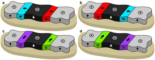 |
| These schematics of magnetic domain walls in perpendicularly magnetized thin films show (a) left-handed and (b) right-handed Neel-type walls; and (c) left-handed and (d) right-handed Bloch-type walls. The directions of the arrows correspond to the magnetization direction.
|
|
The study was carried out at at the National Center for Electron Microscopy (NCEM), which is part of the Molecular Foundry, a DOE Office of Science User Facility. The results have been reported in a Nature Communications paper ("Unlocking Bloch-type chirality in ultrathin magnets through uniaxial strain").
|
|
Electronic Charge and Spin
|
|
In addition to carrying a negative electrical charge, electrons also carry a quantum mechanical property known as “spin,” which arises from tiny magnetic fields created by their rotational momentum. For the sake of simplicity, spin is assigned a direction of either “up” or “down.” Because of these two properties, a flow of electrons creates both charge and spin currents. Charge currents are well understood and serve as the basis for today’s electronic devices. Spin currents are just beginning to be explored as the basis for the emerging new field of spintronics. Coupling the flows of charge and spin currents together opens the door to yet another new field in electronics called “spin–orbitronics.” The promise of spin-orbitronics is smaller, faster and far more energy efficient devices through solid-state magnetic memory.
|
|
The key to coupling charge and spin currents lies within magnetic domains, regions in a magnetic material in which all of the spins of the electrons are aligned with one another and point in the same direction – up or down. In a magnetic material containing multiple magnetic domains, individual domains are separated from one another by narrow zones or “walls” that feature rapidly changing spin directions. There are two types of magnetic domain walls known to exist in magnetic thin films: Bloch, in which electron spin rotates like a helical spiral around an axis; and Neel, in which electron spin rotates like a cycloidal spiral. Both types of walls can have either right-handed or left-handed chirality.
|
|
Applying a technique called SPLEEM, for Spin-Polarized Low Energy Electron Microscopy, to a thin-film of iron/nickel bilayers on tungsten, Chen and Schmid and their collaborators were able to stabilize domain walls that were a mixture of Bloch and Neel types. They also showed how the chirality of domain walls can be switched between left-and right-handedness. This was accomplished by controlling uniaxial strain on the thin films in the presence of an asymmetric magnetic exchange interaction between neighbouring electron spins.
|
|
“Depending on their handedness, Neel-type walls are propelled with or against the current direction, while Bloch-type walls are propelled to the left or to the right across the current,” Chen says. “Our findings introduce Bloch-type chirality as a new spin texture and might allow us to tailor the spin structure of chiral domain walls. This would present new opportunities to design spin–orbitronic devices.”
|
|
A key to the success of Chen, Schmid and their colleagues was their SPLEEM imaging technique, which in this country could only be carried out at the Molecular Foundry’s NCEM.
|
|
“Magnetization is a 3D vector, not just a scalar property and in order to see spin textures, the three Cartesian components of the magnetization must be resolved,” Schmid says. “Berkeley Lab’s SPLEEM instrument is one of a mere handful of instruments worldwide that permit imaging all three Cartesian components of magnetization. It was the unique SPLEEM experimental capability that made this spin-orbitronics research possible.”
|

