Physicists develop a cooling system for the processors of the future (w/video)
(Nanowerk News) Researchers from Moscow Institute of Physics and Technology (MIPT) have found a solution to the problem of overheating of active plasmonic components. These components will be essential for high-speed data transfer within the optoelectronic microprocessors of the future, which will be able to function tens of thousands of times faster than the microprocessors currently in use today. In the paper published in ACS Photonics ("Self-Heating and Cooling of Active Plasmonic Waveguides") the researchers have demonstrated how to efficiently cool optoelectronic chips using industry-standard heatsinks in spite of high heat generation in active plasmonic components.
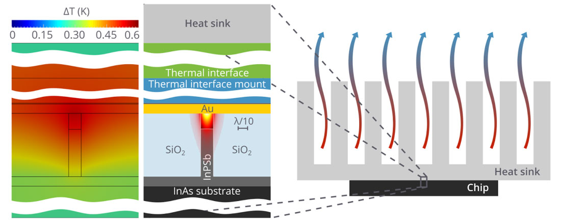
Temperature distribution in an active plasmonic waveguide on an optoelectronic chip with a cooling system. (click on image to enlarge)
The speed of multicore and manycore microprocessors, which are already used in high-performance computer systems, depends not so much on the speed of an individual core, but rather on the time it takes for data to be transferred between the cores. The electrical copper interconnects used in microprocessors today are fundamentally limited in bandwidth, and they cannot be used to maintain the continuing growth of the processor performance. In other words, doubling the number of cores will not double the processing power.
Leading companies in the semiconductor industry, such as IBM, Oracle, Intel, and HP, see the only solution to this problem in switching from electronics to photonics, and they are currently investing billions of dollars into this. Replacing electrons with photons will mean that large amounts of data will be able to be transferred between processor cores almost instantly, which in turn will mean that the processor performance will be nearly proportional to the number of cores.
However, due to diffraction, photonic components are not as easy to scale down as electronic components. Their dimensions cannot be smaller than the size approximately equal to the light wavelength (~ 1 micrometer or 1000 nanometers), but transistors will soon be as small as 10 nanometers. This fundamental problem can be solved by switching from bulk waves to surface waves, which are known as surface plasmon polaritons (SPPs). This will enable to confine light on the nanoscale.
Along with the leading research centers of industrial companies and the laboratories of leading universities, Russian scientists from the Laboratory of Nanooptics and Plasmonics of MIPT’s Center of Nanoscale Optoelectronics are also making good progress in this field.
Dmitry Fedyanin and Andrey Vyshnevyy explain their work.
The main difficulty that scientists face is the fact that SPPs are absorbed by metal, which is a key material in plasmonics. This effect is similar to resistance in electronics, where the energy of electrons is lost and converted into heat when current passes through a resistor. The SPP loss can be compensated by pumping additional energy into the SPPs.
However, this pumping will produce additional heat, which in turn will cause an increase in temperature not only in the plasmonic components, but also in the processor as a whole. The higher absorption in the metal, the greater the loss, and the stronger pumping will be required. This raises the temperature, which again causes a loss increase and makes it more difficult to create optical gain, which is required to compensate for the loss, and this means that more powerful pumping is required. A cycle is formed in which the temperature can rise to such an extent that a processor chip simply burns out. This is no surprise, since the heating power per surface unit of the active plasmonic waveguide with loss compensation exceeds 10 kW/cm2, which is twice as high as the intensity of solar radiation at the surface of the Sun!
Dmitry Fedyanin and Andrey Vyshnevyy, researchers at MIPT’s Laboratory of Nanooptics and Plasmonics, have found a solution to this problem. They have demonstrated that using high-performance thermal interfaces, i.e. layers of thermally conductive materials placed between the chip and the cooling system to ensure efficient heat removal from the chip, (thermal grease is a popular type of thermal interface, although it is not very efficient) high-performance optoelectronic chips can be cooled using conventional cooling systems.
Based on the results of numerical simulations, Fedyanin and Vyshnevyy concluded that if an optoelectronic chip with active plasmonic waveguides is placed in air, its temperature will increase by several hundred degrees Celsius, which will cause the device to malfunction. Multi-layered thermal interfaces of nano- and micrometer thickness combined with simple cooling systems can reduce the temperature of the chip from several hundred degrees to approximately ten degrees with respect to the ambient temperature. This opens the prospects for the implementation of high-performance optoelectronic microprocessors in a wide range of applications, ranging from supercomputers to compact electronic devices.
Source: Moscow Institute of Physics and Technology