| Posted: Sep 25, 2018 |
Multimodal imaging shows strain can drive chemistry in a photovoltaic material(Nanowerk News) A unique combination of imaging tools and atomic-level simulations has allowed a team led by the Department of Energy’s Oak Ridge National Laboratory to solve a longstanding debate about the properties of a promising material that can harvest energy from light. |
| The researchers used multimodal imaging to “see” nanoscale interactions within a thin film of hybrid organic–inorganic perovskite, a material useful for solar cells. They determined that the material is ferroelastic, meaning it can form domains of polarized strain to minimize elastic energy. This finding was contrary to previous assumptions that the material is ferroelectric, meaning it can form domains of polarized electric charge to minimize electric energy. |
| “We found that people were misguided by the mechanical signal in standard electromechanical measurements, resulting in the misinterpretation of ferroelectricity,” said Yongtao Liu of ORNL, whose contribution to the study became a focus of his PhD thesis at the University of Tennessee, Knoxville (UTK). |
| Olga Ovchinnikova, who directed the experiments at ORNL’s Center for Nanophase Materials Sciences (CNMS), added, “We used multimodal chemical imaging—scanning probe microscopy combined with mass spectrometry and optical spectroscopy—to show that this material is ferroelastic and how the ferroelasticity drives chemical segregation.” |
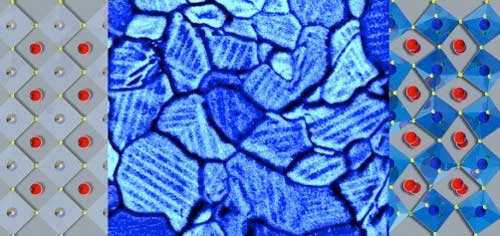 |
| In a thin film of a solar-energy material, molecules in twin domains (modeled in left and right panels) align in opposing orientations within grain boundaries (shown by scanning electron microscopy in the center panel). Strain can change chemical segregation and may be engineered to tune photovoltaic efficiency. (Image: Stephen Jesse/Oak Ridge National Laboratory) |
| The findings, reported in Nature Materials ("Chemical nature of ferroelastic twin domains in CH3NH3PbI3 perovskite"), revealed that differential strains cause ionized molecules to migrate and segregate within regions of the film, resulting in local chemistry that may affect the transport of electric charge. |
| The understanding that this unique suite of imaging tools enables allows researchers to better correlate structure and function and fine-tune energy-harvesting films for improved performance. |
| “We want to predictively make grains of particular sizes and geometries,” Liu said. “The geometry is going to control the strain, and the strain is going to control the local chemistry.” |
| For their experiment, the researchers made a thin film by spin-casting a perovskite on an indium tin oxide–coated glass substrate. This process created the conductive, transparent surface a photovoltaic device would need—but also generated strain. To relieve the strain, tiny ferroelastic domains formed. One type of domain was “grains,” which look like what you might see flying over farmland with patches of different crops skewed in relation to one another. Within grains, sub-domains formed, similar to rows of two plant types alternating in a patch of farmland. These adjacent but opposing rows are “twin domains” of segregated chemicals. |
| The technique that scientists previously used to claim the material was ferroelectric was piezoresponse force microscopy (“piezo” means “pressure), in which the tip of an atomic force microscope (AFM) measures a mechanical displacement due to its coupling with electric polarization—namely, electromechanical displacement. |
| “But you’re not actually measuring the true displacement of the material,” Ovchinnikova warned. “You’re measuring the deflection of this whole ‘diving board’ of the cantilever.” Therefore, the researchers used a new measurement technique to separate cantilever dynamics from displacement of the material due to piezoresponse—the Interferometric Displacement Sensor (IDS) option for the Cypher AFM, developed by co-author Roger Proksch, CEO of Oxford Instruments Asylum Research. They found the response in this material is from cantilever dynamics alone and is not a true piezoresponse, proving the material is not ferroelectric. |
| “Our work shows the effect believed due to ferroelectric polarization can be explained by chemical segregation,” Liu said. |
| The study’s diverse microscopy and spectroscopy measurements provided experimental data to validate atomic-level simulations. The simulations bring predictive insights that could be used to design future materials. |
| “We’re able to do this because of the unique environment at CNMS where we have characterization, theory and synthesis all under one roof,” Ovchinnikova said. “We didn’t just utilize mass spectrometry because [it] gives you information about local chemistry. We also used optical spectroscopy and simulations to look at the orientation of the molecules, which is important for understanding these materials. Such a cohesive chemical imaging capability at ORNL leverages our functional imaging.” |
| Collaborations with industry allow ORNL to have unique tools available for scientists, including those that settled the debate about the true nature of the light-harvesting material. For example, an instrument that uses helium ion microscopy (HIM) to remove and ionize molecules was coupled with a secondary ion mass spectroscopy (SIMS) to identify molecules based on their weights. The HIM-SIMS instrument ZEISS ORION NanoFab was made available to ORNL from developer ZEISS for beta testing and is one of only two such instruments in the world. Similarly, the IDS instrument from Asylum Research, which is a laser Doppler vibrometer, was also made available to ORNL for beta testing and is the only one in existence. |
| “Oak Ridge National Laboratory researchers are naturally a good fit for working with industry because they possess unique expertise and are able to first use the tools the way they're meant to,” said Proksch of Asylum. “ORNL has a facility [CNMS] that makes instruments and expertise available to many scientific users who can test tools on different problems and provide strong feedback during beta testing as vendors develop and improve the tools, in this case our new IDS metrological AFM.” |
| Source: Oak Ridge National Laboratory |
|
Subscribe to a free copy of one of our daily Nanowerk Newsletter Email Digests with a compilation of all of the day's news. |

