| Posted: Oct 16, 2018 |
Blue phosphorus - mapped and measured for the first time(Nanowerk News) Until recently, the existence of "blue" phosphorus was pure theory: Now a Helmholtz Zentrum Berlin (HZB) team was able to examine samples of blue phosphorus at BESSY II for the first time and confirm via mapping of their electronic band structure that this is actually this exotic phosphorus modification. Blue phosphorus is an interesting candidate for new optoelectronic devices. The results have been published in Nano Letters ("Band renormalization of blue phosphorus on Au(111)"). |
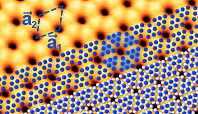 |
| The STM image shows blue phosphorus on a gold substrate. The calculated atomic positions of the slightly elevated P atoms are shown in blue, the lower lying ones in white. Groups of six elevated P atoms appear as triangles. (Image: HZB) |
| The element phosphorus can exist in various allotropes and changes its properties with each new form. So far, red, violet, white and black phosphorus have been known. While some phosphorus compounds are essential for life, white phosphorus is poisonous and inflammable and black phosphorus - on the contrary - particularly robust. |
| Now, another allotrope has been identified: In 2014, a team from Michigan State University, USA, performed model calculations to predict that "blue phosphorus" should be also stable. In this form, the phosphorus atoms arrange in a honeycomb structure similar to graphene, however, not completely flat but regularly "buckled". |
| Model calculations showed that blue phosphorus is not a narrow gap semiconductor like black phosphorus in the bulk but possesses the properties of a semiconductor with a rather large band gap of 2 electron volts. This large gap, which is seven times larger than in bulk black phosphorus, is important for optoelectronic applications. |
Blue P examined at BESSY II |
| In 2016, blue phosphorus was successfully stabilized on a gold substrate by evaporation. Nevertheless, only now we know for certain that the resulting material is indeed blue phosphorus. To this end, a team from HZB around Evangelos Golias has probed the electronic band structure of the material at BESSY II. They were able to measure by angle-resolved photoelectron spectroscopy the distribution of electrons in its valence band, setting the lower limit for the band gap of blue phosphorus. |
Band structure influenced by the substrate |
| They found that the P atoms do not arrange independently of the gold substrate but try to adjust to the spacings of the Au atoms. This distorts the corrugated honeycomb lattice in a regular manner which in turn affects the behavior of electrons in blue phosphorus. |
| As a result, the top of the valence band that defines the one end of the semiconducting band gap agrees with the theoretical predictions about its energy position but is somewhat shifted. |
Outlook: optoelectronic applications |
| "So far, researchers have mainly used bulk black phosphorus to exfoliate atomically thin layers", Prof. Oliver Rader, head of HZB-Department Materials for green spintronics explains. "These also show a large semiconducting band gap but do not possess the honeycomb structure of blue phosphorus and, above all, cannot be grown directly on a substrate. Our work not only reveals all the material properties of this novel two-dimensional phosphorus allotrope but highlights the impact of the supporting substrate on the behavior of electrons in blue phosphorus, an essential parameter for any optoelectronic application." |
| Source: Helmholtz Zentrum Berlin |
|
Subscribe to a free copy of one of our daily Nanowerk Newsletter Email Digests with a compilation of all of the day's news. |

