| Feb 11, 2020 |
'Atomic dance' reveals new insights into performance of 2D materials(Nanowerk News) A team of Northwestern University materials science researchers have developed a new method to view the dynamic motion of atoms in atomically thin 2D materials. The imaging technique, which reveals the underlying cause behind the performance failure of a widely used 2D material, could help researchers develop more stable and reliable materials for future wearables and flexible electronic devices. |
| These 2D materials - such as graphene and borophene - are a class of single-layer, crystalline materials with widespread potential as semiconductors in advanced ultra-thin, flexible electronics. Yet due to their thin nature, the materials are highly sensitive to external environments, and have struggled to demonstrate long-term stability and reliability when utilized in electronic devices. |
| "Atomically thin 2D materials offer the potential to dramatically scale down electronic devices, making them an attractive option to power future wearable and flexible electronics," said Vinayak Dravid, Abraham Harris Professor of Materials Science and Engineering at the McCormick School of Engineering. |
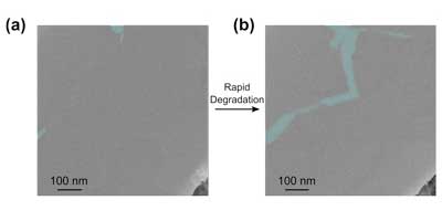 |
| An image of void coalescence. On left, a low-magnification TEM of MoS2 grain boundary region prior to biasing. On right, the same region after an electrical bias is applied. As is apparent, neighboring voids (blue) appear to coalesce to form porous chains. (Image: Northwestern University) |
| The study was published in the journal ACS Nano ("Direct Visualization of Electric Field induced Structural Dynamics in Monolayer Transition Metal Dichalcogenides"). Dravid is the corresponding author on the paper. Chris Wolverton, the Jerome B. Cohen Professor of Materials Science and Engineering, also contributed to the research. |
| "Unfortunately, electronic devices now operate as a kind of 'black box.' Although device metrics can be measured, the motion of single atoms within the materials responsible for these properties is unknown, which greatly limits efforts to improve performance," added Dravid, who serves as director of the Northwestern University Atomic and Nanoscale Characterization (NUANCE) Center. The research allows a way to move past that limitation with a new understanding of the structural dynamics at play within 2D materials receiving electrical voltage. |
| Building upon a previous study in which the researchers used a nanoscale imaging technique to observe failure in 2D materials caused by heat, the team used a high-resolution, atomic-scale imaging method called electron microscopy to observe the movement of atoms in molybdenum disulfide (MoS2), a well-studied material originally used as a dry lubricant in greases and friction materials that has recently gained interest for its electronic and optical properties. When the researchers applied an electric current to the material, they observed its highly mobile sulfur atoms move continuously to vacant areas in the crystalline material, a phenomenon they dubbed, "atomic dance." |
| That movement, in turn, caused the MoS2's grain boundaries -- a natural defect created in the space where two crystallites within the material meet-- to separate, forming narrow channels for the current to travel through. |
| "As these grain boundaries separate, you are left with only a couple narrow channels, causing the density of the electrical current through these channels to increase," said Akshay Murthy, a PhD student in Dravid's group and the lead author on the study. "This leads to higher power densities and higher temperatures in those regions, which ultimately leads to failure in the material." |
| "It's powerful to be able to see exactly what's happening on this scale," Murthy continued. "Using traditional techniques, we could apply an electric field to a sample and see changes in the material, but we couldn't see what was causing those changes. If you don't know the cause, it's difficult to eliminate failure mechanisms or prevent the behavior going forward." |
| With this new way to study 2D materials at the atomic level, the team believes researchers could use this imaging approach to synthesize materials that are less susceptible to failure in electronic devices. In memory devices, for example, researchers could observe how regions where information is stored evolve as electric current is applied and adapt how those materials are designed for better performance. |
| The technique could also help improve a host of other technologies, from transistors in bioelectronics to light emitting diodes (LEDs) in consumer electronics to photovoltaic cells that comprise solar panels. |
| "We believe the methodology we have developed to monitor how 2D materials behave under these conditions will help researchers overcome ongoing challenges related to device stability," Murthy said. "This advance brings us one step closer to moving these technologies from the lab to the marketplace." |
| Source: Northwestern University |
|
Subscribe to a free copy of one of our daily Nanowerk Newsletter Email Digests with a compilation of all of the day's news. |

