| Feb 18, 2020 |
Creating custom light using 2D materials(Nanowerk News) Finding new semi-conductor materials that emit light is essential for developing a wide range of electronic devices. But making artificial structures that emit light tailored to our specific needs is an even more attractive proposition. However, light emission in a semi-conductor only occurs when certain conditions are met. |
| Researchers from the University of Geneva (UNIGE), Switzerland, in collaboration with the University of Manchester, have discovered an entire class of two-dimensional materials that are the thickness of one or a few atoms. When combined together, these atomically thin crystals are capable of forming structures that emit customisable light in the desired colour. |
| This research, published in the journal Nature Materials ("Design of van der Waals Interfaces for Broad-Spectrum Optoelectronics"), marks an important step towards the future industrialisation of two-dimensional materials. |
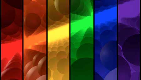 |
| Artistic view of a junction of different 2D light-emitting materials. (Image: Xavier Ravinet) |
| Semi-conductor materials capable of emitting light are used in sectors as diverse as telecommunications, light emitting devices (LEDs) and medical diagnostics. Light emission occurs when an electron jumps inside the semi-conductor from a higher energy level to a lower level. It is the difference in energy that determines the colour of the emitted light. |
| For light to be produced, the velocity of the electron before and after the jump must be exactly the same, a condition that depends on the specific semiconducting material considered. Only some semi-conductors can be used for light emission: for example, silicon – used to make our computers – cannot be employed for manufacturing LEDs. |
| “We asked ourselves whether two-dimensional materials could be used to make structures that emit light with the desired colour”, explains Alberto Morpurgo, a professor in the Department of Quantum Matter Physics, at the UNIGE Faculty of Science. |
| Two-dimensional materials are perfect crystals which, like graphene, are one or a few atoms thick. Thanks to recent technical advances, different two-dimensional materials can be stacked on top of each other to form artificial structures that behave like semi-conductors. The advantage of these “artificial semi-conductors” is that the energy levels can be controlled by selecting the chemical composition and thickness of the materials that make up the structure. |
“Artificial semi-conductors of this kind were made for the first time only two or three years ago”, explains Nicolas Ubrig, a researcher in the team led by professor Morpurgo. “When the two-dimensional materials have exactly the same structure and their crystals are perfectly aligned, this type of artificial semi-conductor can emit light. But it’s very rare.” These conditions are so strict that they leave little freedom to control the light emitted.
Custom light“Our objective was to manage to combine different two-dimensional materials to emit light while being free from all constraints”, continues professor Morpurgo. |
| The physicists thought that, if they could find a class of materials where the velocity of the electrons before and after the change in energy level was zero, it would be an ideal scenario which would always meet the conditions for light emission, regardless of the details of the crystal lattices and their relative orientation. |
| A large number of known two-dimensional semi-conductors have a zero-electron velocity in the relevant energy levels. Thanks to this diversity of compounds, many different materials can be combined, and each combination is a new artificial semi-conductor emitting light of a specific colour. |
| “Once we had the idea, it was easy to find the materials to use to implement it”, adds professor Vladimir Fal’ko from the University of Manchester. |
| Materials that were used in the research included various transition metal dichalcogenides (such as MoS2, MoSe2 and WS2) and InSe. Other possible materials have been identified and will be useful for widening the range of colours of the light emitted by these new artificial semi-conductors. |
Tailor-made light for mass industrialisation |
| “The great advantage of these 2D materials, thanks to the fact that there are no more preconditions for the emission of light, is that they provide new strategies for manipulating the light as we see fit, with the energy and colour that we want to have”, continues Ubrig. |
| This means it is possible to devise future applications on an industrial level, since the emitted light is robust and there is no longer any need to worry about the alignment of atoms. |
| Source: Université de Genève |
|
Subscribe to a free copy of one of our daily Nanowerk Newsletter Email Digests with a compilation of all of the day's news. |

