| Oct 15, 2020 |
Altering the properties of 2D materials at the nanometer scale
(Nanowerk News) Materials all come with their own set of properties – they can be insulating, semi-conducting, metallic, transparent or flexible, for example. Some combine several very useful properties, which is the case for 2D materials. Made up of just one or few layers of atoms, these materials are highly promising for the manufacture of next-generation electronic and optoelectronic devices.
|
|
“In our field, silicon is still king. But it’s reaching its limits for some electronic devices, like those that need to be flexible or transparent. 2D materials could be a viable alternative,” says Jürgen Brugger, the professor who heads the Microsystems Laboratory 1 at EPFL’s School of Engineering.
|
Customizing properties for specific applications
|
|
Before 2D materials can be used, they need to be structured, which means cutting them into the right size and shape for the given application. Their physical properties (such as the bandgap) also need to be adjusted, both throughout the material and at specific locations.
|
|
Scientists at the Microsystems Laboratory 1, working in association with ETH Zurich and IBM, have developed a new method for altering the properties of these materials.
|
Deforming materials with a nanometric tip
|
|
The research team used thermal scanning probe lithography (t-SPL), which entails placing a heated nanometric tip on the material and exerting pressure to create the desired shape – in this case, wavy – while carefully controlling the force and temperature.
|
|
“Several methods already exist for deforming 2D materials globally and locally. But our thermo-mechanic approach can create larger deformations and therefore produce wider variations in a material’s physical properties,” says Ana Conde-Rubio, a scientist at the EPFL lab. More specifically, the new method can change the energy gap between the valence band and conduction band, consequently altering the material’s electronic and optical properties. And this change in bandgap can be performed locally with a spatial resolution down to 20 nanometers.
|
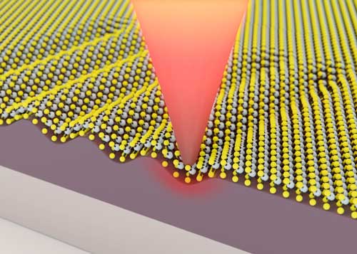 |
| A heated nanometric tip deforms the material to changes its properties. (Image: Samuel Howell)
|
A single tool for cutting and modifying 2D materials
|
|
The scientists had already developed a method for cutting 2D materials with high precision. Now their aim is to combine that method with this new way of changing the material’s properties. “Using the same tool, the t-SPL, we will be able to manufacture devices with the desired shape, dimensions and physical properties, with a resolution down to the 10 nanometers scale” says Xia Liu, another scientist at Brugger’s lab.
|
|
The team’s findings have been published in Nano Letters ("Thermo-mechanical Nanostraining of Two-Dimensional Materials").
|
|
Their work forms part of a larger research project to develop new processes for manufacturing and modifying polymer materials for wearables and implantables. The goal is to enable the transition from lab-scale to industrial-scale production of next-generation devices.
|

