| Mar 19, 2021 |
Building tough synthetic nanomaterials with DNA nanotechnology
(Nanowerk News) Columbia Engineering researchers, working with Brookhaven National Laboratory, report today that they have built designed nanoparticle-based 3D materials that can withstand a vacuum, high temperatures, high pressure, and high radiation.
|
|
This new fabrication process results in robust and fully engineered nanoscale frameworks that not only can accommodate a variety of functional nanoparticle types but also can be quickly processed with conventional nanofabrication methods.
|
|
“These self-assembled nanoparticles-based materials are so resilient that they could fly in space,” says Oleg Gang, professor of chemical engineering and of applied physics and materials science, who led the study published by Science Advances ("Resilient three-dimensional ordered architectures assembled from nanoparticles by DNA"). “We were able to transition 3D DNA-nanoparticle architectures from liquid state—and from being a pliable material—to solid state, where silica re-enforces DNA struts. This new material fully maintains its original framework architecture of DNA-nanoparticle lattice, essentially creating a 3D inorganic replica. This allowed us to explore—for the first time—how these nanomaterials can battle harsh conditions, how they form, and what their properties are.”
|
|
Material properties are different at the nanoscale and researchers have long been exploring how to use these tiny materials – 1 000 to 10 000 times smaller than the thickness of a human hair – in all kinds of applications, from making sensors for phones to building faster chips for laptops. Fabrication techniques, however, have been challenging in realizing 3D nano-architectures.
|
|
DNA nanotechnology enables the creation of complexly organized materials from nanoparticles through self-assembly, but given the soft and environment-dependent nature of DNA, such materials might be stable under only a narrow range of conditions.
|
|
In contrast, the newly formed materials can now be used in a broad range of applications where these engineered structures are required. While conventional nanofabrication excels in creating planar structures, Gang’s new method allows for fabrication of 3D nanomaterials that are becoming essential to so many electronic, optical, and energy applications.
|
|
Gang, who holds a joint appointment as group leader of the Soft and Bio Nanomaterials Group at Brookhaven Lab’s Center for Functional Nanomaterials, is at the forefront of DNA nanotechnology, which relies on folding DNA chain into desired two and three-dimensional nanostructures. These nanostructures become building blocks that can be programmed via Watson-Crick interactions to self-assemble into 3D architectures.
|
|
His group designs and forms these DNA nanostructures, integrates them with nanoparticles and directs the assembly of targeted nanoparticle-based materials. And, now, with this new technique, the team can transition these materials from being soft and fragile to solid and robust.
|
|
This new study demonstrates an efficient method for converting 3D DNA-nanoparticle lattices into silica replicas, while maintaining the topology of the interparticle connections by DNA struts and the integrity of the nanoparticle organization. Silica works well because it helps retain the nanostructure of the parent DNA lattice, forms a robust cast of the underlying DNA and does not affect nanoparticles arrangements.
|
|
“The DNA in such lattices takes on the properties of silica,” says Aaron Michelson, a PhD student from Gang’s group. “It becomes stable in air and can be dried and allows for 3D nanoscale analysis of the material for the first time in real space. Moreover, silica provides strength and chemical stability, it’s low-cost and can be modified as needed—it’s a very convenient material.”
|
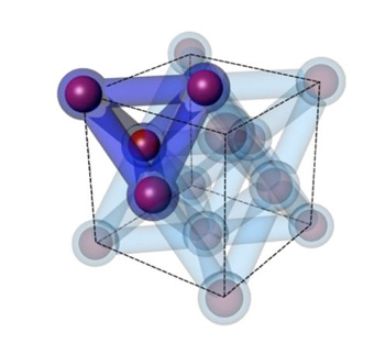 |
| Mineralization of 3D lattice formed by DNA tetrahedra (about 30 nm) and gold nanoparticle into all-inorganic 3D silica-Au replicas with preserved architecture. (Image: Oleg Gang, Columbia Engineering)
|
|
To learn more about the properties of their nanostructures, the team exposed the converted to silica DNA-nanoparticles lattices to extreme conditions: high temperatures above 10 000 °C and high mechanical stresses over 8GPa (about 80,000 times more than atmosphere pressure, or 80 times more than at the deepest ocean place, the Mariana trench), and studied these processes in-situ. To gauge the structures’ viability for applications and further processing steps, the researchers also exposed them to high doses of radiation and focused ion beams.
|
|
“Our analysis of the applicability of these structures to couple with traditional nanofabrication techniques demonstrates a truly robust platform for generating resilient nanomaterials via DNA-based approaches for discovering their novel properties,” Gang notes. “This is a big step forward, as these specific properties mean that we can use our 3D nanomaterial assembly and still access the full range of conventional materials processing steps. This integration of novel and conventional nanofabrication methods is needed to achieve advances in mechanics, electronics, plasmonics, photonics, superconductivity, and energy materials.”
|
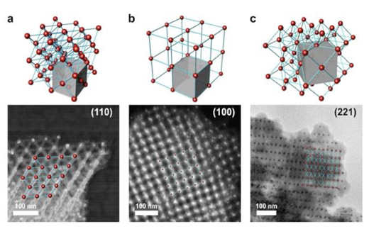 |
| Different types of nanoscale lattices formed with polyhedra DNA nano-frames (tetrahedra, cubes, and octahedra) and gold nanoparticle are mineralized with controllable silica coating thicknesses (from about 5nm to a full space-filling). (Image: Oleg Gang, Columbia Engineering)
|
|
Collaborations based on Gang’s work have already led to novel superconductivity and conversion of the silica to conductive and semiconductive media for further processing. These include an earlier study published by Nature Communications ("DNA-assembled superconducting 3D nanoscale architectures") and one recently published by Nano Letters ("Engineered Silicon Carbide Three-Dimensional Frameworks through DNA-Prescribed Assembly").
|
|
The researchers are also planning to modify the structure to make a broad range of materials with highly desirable mechanical and optical properties.
|
|
“Computers have been made with silicon for over 40 years,” Gang adds. “It took four decades to push the fabrication down to about 10 nm for planar structures and devices. Now we can make and assemble nanoobjects in a test tube in a couple of hours without expensive tools. Eight billion connections on a single lattice can now be orchestrated to self-assemble through nanoscale processes that we can engineer. Each connection could be a transistor, a sensor, or an optical emitter—each can be a bit of data stored. While Moore’s law is slowing, the programmability of DNA assembly approaches is there to carry us forward for solving problems in novel materials and nanomanufacturing. While this has been extremely challenging for current methods, it is enormously important for emerging technologies.”
|

