Precision machining produces tiny, light-guiding nanocubes for advancing info tech (w/video)
(Nanowerk News) Drilling with the beam of an electron microscope, scientists at the Department of Energy’s Oak Ridge National Laboratory precisely machined tiny electrically conductive cubes that can interact with light and organized them in patterned structures that confine and relay light’s electromagnetic signal. This demonstration is a step toward potentially faster computer chips and more perceptive sensors.
The seeming wizardry of these structures comes from the ability of their surfaces to support collective waves of electrons, called plasmons, with the same frequency as light waves but with much tighter confinement. The light-guiding structures are measured in nanometers.
“These nanoscale cube systems allow extreme confinement of light in specific locations and tunable control of its energy,” said ORNL’s Kevin Roccapriore, first author of a study published in the journal Small ("Sculpting the plasmonic responses of nanoparticles by directed electron beam irradiation"). “It’s a way to connect signals with very different length scales.”
The feat may prove critical for quantum and optical computing. Quantum computers encode information with quantum bits, or qubits, determined by a quantum state of a particle, such as its spin. Qubits can store many values compared with the single value stored by a classical bit.
Light — electromagnetic radiation that propagates by massless elementary particles called photons — replaces electrons as the messenger in optical computers. Because photons travel faster than electrons and do not generate heat, optical computers could have performance and energy efficiency superior to classical computers.
Future technologies may use the best of both worlds.
“Light is the preferred way to communicate with qubits, but you cannot connect contacts to them directly,” said senior author Sergei Kalinin of ORNL. “The problem with visible light is its wavelengths range from about 380 nanometers for violet to around 700 nanometers for red. That’s too big because we want to make devices only a few nanometers in size. This work aims to create a framework to move technology beyond Moore’s law and classical electronics. If you try to put ‘light’ and ‘small’ together, that’s exactly where plasmonics comes into play.”
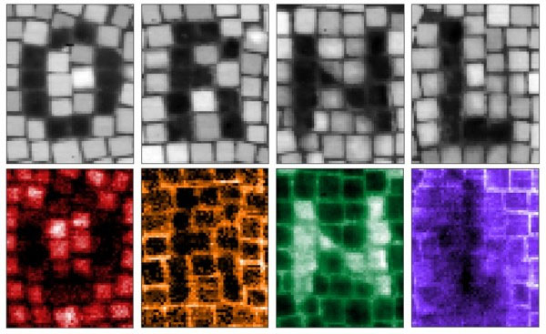
ORNL scientists used an electron beam for precision machining of nanoscale materials. Cubes were milled to change their shape and could also be removed from an array. (Image: Kevin Roccapriore/ORNL)
And if there’s a great future in plasmonics, the ORNL-led achievement may help overcome a signal size mismatch that threatens the integration of components made of different materials. Those hybrid components will need to “talk” to each other in next-generation optoelectronic devices. Plasmonics may bridge the gap.
Plasmonic phenomena were first observed in metals, which are conductive because of their free electrons. The ORNL team used cubes made of a transparent semiconductor that behaves like a metal — indium oxide doped with tin and fluorine.
The fact that the cube is a semiconductor is the key to its energy tunability. The energy of a light wave is related to its frequency. The higher the frequency, the shorter the wavelength. Wavelengths of visible light appear to the human eye as colors. Because a semiconductor can be doped — that is, a small impurity can be added — its wavelength can be shifted on the spectrum.
The study’s cubes were each 10 nanometers wide, which is much smaller than the wavelength of visible light. Synthesized at the University of Texas at Austin by Shin-Hum Cho and Delia Milliron, the cubes were placed in a detergent to prevent clumping and pipetted onto a substrate, where they self-assembled into a two-dimensional array. A shell of detergent surrounded each cube, spacing them apart evenly. After the detergent was removed, the arrays were sent to ORNL.
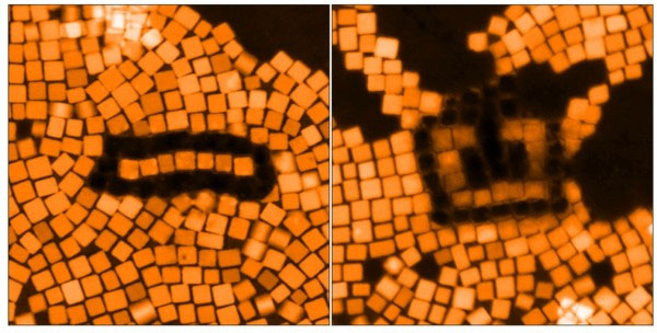
“That the cubes do not directly touch is important for the collective behavior,” said Roccapriore, who organized the cubes into diverse structures. “Each cube individually has its own plasmon behavior. When we bring them together in geometries like a nanowire, they talk to one another and produce new effects that are not typically seen in similar geometries that aren’t made up of individual elements.”
Each cube shown has its own plasmonic behavior. Bring them together in patterns — an antenna, left image, or split ring resonator, right image — and they “talk,” producing unique effects. (Image: Kevin Roccapriore/ORNL)
The study builds on prior work to sculpt three-dimensional structures as small as a nanometer with an electron beam ("New electron microscopy method sculpts 3-D structures at atomic level"). “The current paper proves that the plasmonic effect, as well as the structure, can be sculpted,” Roccapriore said. “At the end of the day, we’re interested in the electron wave — where is it and what is its energy? We’re controlling those two things.”
Kalinin added, “We want to transition from using what exists in nature by chance to fabricating materials with the right responses. We can take a system of cubes, shine light on it and channel energy into small volumes localized exactly where we want them to be.”
The project was a natural for Roccapriore, who conducted a lot of electron-beam lithography in graduate school and even built a machine in his garage to make and mill 3D-printed structures. At ORNL, experimenting with the beam of an electron microscope, he adjusted its current to intentionally shift from imaging to modification mode. He found he could remove bits of cubes or entire cubes from an array to make patterned objects at will. He also discovered that, just like addition of chemical elements enables tuning of cube energies, so too does selective removal of chemical elements. Such atomic precision is possible with scanning transmission electron microscopy, or STEM.
The key to characterizing plasmonic behavior within single cubes and among collective cube assemblies was a technique called electron energy loss spectroscopy. It uses a STEM instrument with an electron beam filtered to energies within a narrow range. The beam loses energy as its electrons pass through the sample, interact with electrons in the material and transfer a little energy to the system by exciting plasmons.
“Electron energy loss spectroscopy provides deep insights into exotic physics and quantum phenomena related to plasmonic behavior,” said co-author Andrew Lupini of ORNL, who helped map the energies of electrons in the cubes and arrays of cubes. Lupini is one of the developers of aberration-corrected STEM, which made pioneering advances possible. “Electron energy loss spectroscopy lets us analyze evolving plasmonic responses in real time as the cubes are sculpted. We can figure out relationships between arrangements of cubes and their plasmonic properties.”
The scientists plan to create a library of relationships between materials, structures and plasmonic properties. That new knowledge will provide the foundational understanding needed to eventually mass-produce structures that can direct the flow of light in plasmonic nanocircuits. According to Roccapriore, “the idea is to understand the relationships using machine learning and then automate the process.”