| Jun 08, 2022 |
Scientists observe effects of heat in materials with atomic resolution
(Nanowerk News) As electronic, thermoelectric and computer technologies have been miniaturized to nanometer scale, engineers have faced a challenge studying fundamental properties of the materials involved; in many cases, targets are too small to be observed with optical instruments.
|
|
Using cutting-edge electron microscopes and novel techniques, a team of researchers at the University of California, Irvine, the Massachusetts Institute of Technology and other institutions has found a way to map phonons – vibrations in crystal lattices – in atomic resolution, enabling deeper understanding of the way heat travels through quantum dots, engineered nanostructures in electronic components.
|
|
To investigate how phonons are scattered by flaws and interfaces in crystals, the researchers probed the dynamic behavior of phonons near a single quantum dot of silicon-germanium using vibrational electron energy loss spectroscopy in a transmission electron microscope, equipment housed in the Irvine Materials Research Institute on the UCI campus. The results of the project are the subject of a paper published in Nature ("Nanoscale imaging of phonon dynamics by electron microscopy").
|
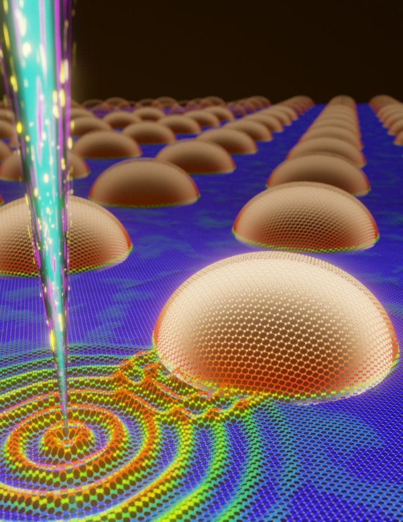 |
| Nanometer-scale quantum dots made of an alloy of silicon and germanium were targeted by researchers at UCI using a technique dubbed “vibrational electron energy loss spectroscopy” in a transmission electron microscope in the Irvine Materials Research Institute. The work resulted in the first atomic-level observation of the way phonons behave in nanoengineered quantum dots. (Image: Chaitanya Gadre, Xingxu Yan, Xiaoqing Pan / UCI)
|
|
“We developed a novel technique to differentially map phonon momenta with atomic resolution, which enables us to observe nonequilibrium phonons that only exist near the interface,” said co-author Xiaoqing Pan, UCI professor of materials science and engineering and physics, Henry Samueli Endowed Chair in Engineering, and IMRI director. “This work marks a major advance in the field because it’s the first time we have been able to provide direct evidence that the interplay between diffusive and specular reflection largely depends on the detailed atomistic structure.”
|
|
According to Pan, at the atomic scale, heat is transported in solid materials as a wave of atoms displaced from their equilibrium position as heat moves away from the thermal source. In crystals, which possess an ordered atomic structure, these waves are called phonons: wave packets of atomic displacements that carry thermal energy equal to their frequency of vibration.
|
|
Using an alloy of silicon and germanium, the team was able to study how phonons behave in the disordered environment of the quantum dot, in the interface between the quantum dot and the surrounding silicon, and around the dome-shaped surface of the quantum dot nanostructure itself.
|
|
“We found that the SiGe alloy presented a compositionally disordered structure that impeded the efficient propagation of phonons,” said Pan. “Because silicon atoms are closer together than germanium atoms in their respective pure structures, the alloy stretches the silicon atoms a bit. Due to this strain, the UCI team discovered that phonons were being softened in the quantum dot due to the strain and alloying effect engineered within the nanostructure.”
|
|
Pan added that softened phonons have less energy, which means that each phonon carries less heat, reducing thermal conductivity as a result. The softening of vibrations is behind one of the many mechanisms of how thermoelectric devices impede the flow of heat.
|
|
One of the key outcomes of the project was the development of a new technique for mapping the direction of the thermal carriers in the material. “This is analogous to counting how many phonons are going up or down and taking the difference, indicating their dominant direction of propagation,” he said. “This technique allowed us to map the reflection of phonons from interfaces.”
|
|
Electronics engineers have succeeded in miniaturizing structures and components in electronics to such a degree that they are now down to the order of a billionth of a meter, much smaller than the wavelength of visible light, so these structures are invisible to optical techniques.
|
|
“Progress in nanoengineering has outpaced advancements in electron microscopy and spectroscopy, but with this research, we are beginning the process of catching up,” said co-author Chaitanya Gadre, a graduate student in Pan’s group at UCI.
|
|
A likely field to benefit from this research is thermoelectrics – material systems that convert heat to electricity. “Developers of thermoelectrics technologies endeavor to design materials that either impede thermal transport or promote the flow of charges, and atom-level knowledge of how heat is transmitted through solids embedded as they often are with faults, defects and imperfections, will aid in this quest,” said co-author Ruqian Wu, UCI professor of physics & astronomy.
|
|
“More than 70 percent of the energy produced by human activities is heat, so it is imperative that we find a way to recycle this back into a useable form, preferably electricity to power humanity’s increasing energy demands,” Pan said.
|

