| Oct 17, 2022 |
Exciton dynamics for future ultra-high-speed communication studied at unprecedented resolution
(Nanowerk News) Future optical communication that's vastly more reliable and faster than what's commonly available today will require new technology. Modern communication is based on charge transfer, which can result in large transmission losses during certain data-intensive applications. Excitons are alternatives, yet they face technical challenges for widespread implementation.
|
|
Now, researchers from Japan have overcome a critical bottleneck that might give rise to ultrafast optical communication technology based on excitons (npj 2D Materials and Applications, "Ultrafast nanoscale exciton dynamics via laser-combined scanning tunnelling microscopy in atomically thin materials").
|
|
Researchers are excited about using excitons – assemblies of bound electrons and holes – for terabits per second optical communication. Unfortunately, rapid exciton dissociation at room temperature in conventional three-dimensional semiconductors precludes immediate practical applications. However, atomically thin layered two-dimensional materials (transition metal dichalcogenides, TMDCs) impart certain advantages.
|
|
For example, in TMDCs, excitons can be stable at room temperature and can travel long distances. Local, ultrasmall-scale defects are inevitable in TMDCs – yet might even be advantageous if researchers can understand the role of such defects on the dynamics of exciton transport, and thus the properties of TMDC-based devices.
|
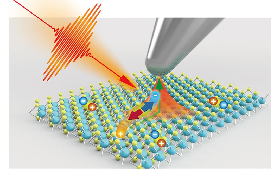 |
| Time-resolved STM (TR-STM) setup for measuring carrier dynamics in transition metal dichalcogenides.(Image: University of Tsukuba
|
|
Understanding the nanoscale dynamics of excitons in TMDCs will help answer such questions. "Commonly used technologies have insufficient resolution," explains Professor Hiroyuki Mogi, lead author, "but our scanning tunneling microscopy approach changes this. To optimize imaging resolution, we applied a bias voltage in a manner that dissociates the underlying excitons, at a resolution of several nanometers."
|
|
The researchers' focus was on how nanostructures – such as grain boundaries and ripples – TMDCs modulated exciton dynamics. A highlight of the research is that grain boundaries corresponded to enhanced exciton recombination within ~8 nanometers. Another highlight is that ripples corresponded to decreased exciton binding energy, and smaller ripples corresponded to a longer exciton lifetime than larger ripples. These results confirm theoretical predictions that prior researchers had been unable to experimentally verify.
|
|
"The 2.5-nanometer spatial resolution of our technique is groundbreaking," says Professor Hidemi Shigekawa, senior author. "At this resolution, we confirmed that in the tungsten diselenide region, the rate of exciton-exciton annihilation was 0.10 ± 0.02 square centimeters per second, and was modulated by local nanostructures."
|
|
Based on the research described here, excitons will become an essential tool to remove many current barriers to remote communication. In the future, that is expected to expand real-life applications of advanced optical communications such as seamless business and financial data-sharing that speeds up operations, faster search-and-rescue operations based on artificial intelligence image-processing of airborne drone data, and safer driverless vehicles.
|

