| Jul 31, 2025 |
New infrared method captures clearer images of nanoscale material structures
A new infrared imaging technique reveals sharp details in nanomaterials like graphene and gold particles by filtering out noise that limits conventional microscopes.
(Nanowerk News) Scientists have developed a new method for capturing high-resolution images of materials just a few atoms thick—without the usual interference that blurs fine details (Microsystems & Nanoengineering, "High-order near-field imaging of low-dimensional materials at infrared wavelengths").
|
|
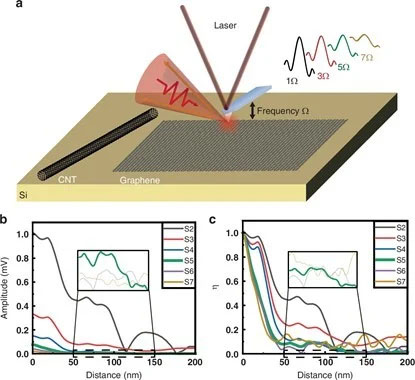
A team at Xi’an Jiaotong University has improved how light is used to reveal the structure of nanoscale materials such as graphene, carbon nanotubes, and gold nanoparticles. Their approach relies on detecting fifth-order near-field optical signals—faint ripples of scattered infrared light that emerge only nanometers above a surface.
|
|
Standard optical microscopes can’t see objects smaller than half the wavelength of visible light. To get around this, scientists use a technique called scattering-type scanning near-field optical microscopy (s-SNOM), which detects scattered light right near the surface. But the method often suffers from background noise that makes it hard to pick out weak signals, especially when examining ultrathin samples.
|
 |
| Schematic of s-SNOM principle and comparison of higher-order signals (2nd–7th). (Image: CAS)
|
|
Previous attempts to reduce this noise, such as using interferometry, added complexity and stability problems. The new method offers a cleaner, more stable alternative by focusing on higher-order light signals—particularly the fifth harmonic, known as S5.
|
|
Using simulations and lab experiments, the researchers showed that infrared light at a wavelength of 1550 nanometers worked best for exciting plasmonic effects in materials like graphene. Plasmons are waves of electrons triggered by light, and tracking them helps scientists understand how materials interact with electromagnetic fields.
|
|
The team demonstrated their technique on a variety of samples. At the interface of graphene and silicon, they captured crisp images of surface plasmons and material boundaries that were invisible with atomic force microscopy (AFM). For multi-walled carbon nanotubes, the method revealed intense light scattering along the tube’s axis—clear evidence of plasmon movement.
|
|
They also tested gold nanoparticles spaced just 10 nanometers apart. AFM showed fuzzy outlines, but the fifth-order signal made the boundaries and gaps much sharper, reducing image distortion from the microscope tip itself.
|
|
“Our approach filters out the background noise that normally masks nanoscale light behavior,” said Professor Shuming Yang, who led the research. “With higher-order signals, we get a clearer picture of how light interacts with these materials—something that’s hard to achieve with conventional methods.”
|
|
Because the technique doesn’t require any physical changes to the sample, it could be integrated into real-time imaging systems or paired with AI tools for automated analysis. It opens up new possibilities for studying 2D materials and nanostructures with exceptional clarity, making it a promising tool for nanophotonics, biosensing, and next-generation optoelectronics.
|

