| Mar 29, 2012 |
Breakthrough in semiconductor structuring
|
|
(Nanowerk News) Microelectronics is no longer imaginable without silicon technology: the material is cheap, readily available and mechanically robust. However, even silicon cannot do everything. Certain materials have properties superior to those of silicon. This is why researchers are looking for ways to unite this element with other semiconductors such as germanium so as to combine and extract the best qualities from the two different materials and to open up new applications.
|
|
However, combining silicon with other semiconductors is not an easy feat. In the past, expensive and time-consuming bonding techniques were needed to combine silicon with devices made from elements of a different composition. "The elegant alternative of monolithic integration is easily done only if the interatomic spacings and thermal properties of silicon and the combination material differ slightly, or if the layers are comparatively thin", says Professor Hans von Känel, Private Docent at ETH Zurich. This is why, until now, there has been no success in constructing thick monolithic layers of germanium on silicon, because defects occur in the crystal lattice. In addition, the silicon wafers warp or the stacks of layers crack under thermal stress, making the electronic components unusable.
|
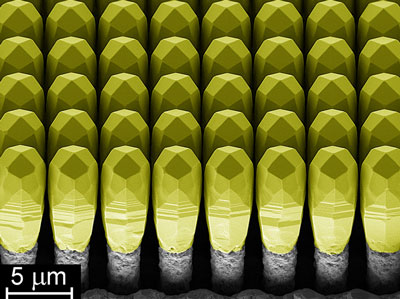 |
| An electron microscope photo of the innovative semiconductor structure: the yellow-coloured heads consist of monolithic germanium and the grey substrate is silicon. (Image: Claudiu Falub, ETH Zurich)
|
|
Breakthrough in semiconductor technology
|
|
The ETH Zurich researchers, led by Hans von Känel and in collaboration with colleagues at the Swiss Centre for Electronics and Microtechnology (CSEM) Neuchâtel, the Politecnico di Milano and the University of Milan-Bicocca, have now found a way to solve this problem. Their paper has just been published in the scientific journal Science ("Scaling Hetero-Epitaxy from Layers to Three-Dimensional Crystals") and is regarded as a breakthrough, which is why it was also chosen as the cover story.
|
|
Instead of a continuous layer of germanium, the Swiss and Italian researchers created a miniaturised "tufted carpet" with tufts consisting of silicon with monolithically structured germanium "grafted on". The spacing between these tufts is only a few dozen nanometres wide. To form them, the scientists etched tiny columns with a side length of two microns and eight microns high into inexpensive silicon substrates. Under extreme conditions, they allowed germanium crystals to grow on these silicon pillars.
|
|
Defect-free germanium layers
|
|
The researchers used this process to generate defect-free silicon-germanium layers or "tufted carpets" that can have almost any desired thickness. The thickest germanium structures so far produced in the laboratory measure 50 microns – ten times thicker than was previously possible. "At this thickness, a continuous layer of germanium would simply flake off", says von Känel. He thinks it is possible to use the new method to generate germanium layers 100 microns thick. The crystal defects that usually occur when layers of differently sized atoms are stacked one on top of another are largely preventable. There is no need for a special technique to bond the materials together.
|
|
The original aim of the research team's work, which forms part of the Nano-Tera project "NEXRAY" with the CSEM, the EMPA and the ETH as partners, and the CSEM as coordinator, was to produce an X-ray detector grown monolithically on the read-out electronics. The detector needs millions of pixels, which must function simultaneously to guarantee high spatial resolution. A layer of germanium at least 50 microns thick is required to ensure sufficient sensitivity. Large-area detectors produced using previous methods are prohibitively expensive. Hans von Känel stresses that "Our research makes it possible to produce the highest-resolution X-ray detector that has ever existed, and at an affordable price".
|
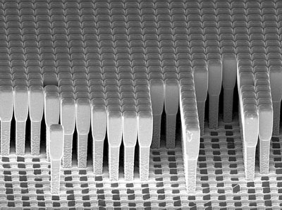 |
| Electron microscope photo of the innovative silicon-germanium structure.
|
|
X-ray radiation reduced
|
|
The high resolution and sensitivity should allow smaller doses of X-rays to be used in future, which could, for example, enable surgical operations to be performed under direct imaging control. This is impossible with present-day X-ray methods because the patient would be exposed to an excessive dose of radiation. However, the ETH Zurich researcher estimates that it will be several more years before an X-ray device based on the new technology comes onto the market.
|
|
However, conceivable applications also include X-ray equipment for baggage screening at airports or for testing electronic components that have already been packaged. It is also possible to manufacture high-efficiency stacked photovoltaic cells made from semiconductors, with each cell absorbing different wavelengths of sunlight. Photocells of this kind are already used in the aerospace industry. Since it will be possible to produce these on silicon wafers in future, the expensive, fragile and heavy germanium substrates could be replaced by cheaper, lighter and mechanically robust silicon substrates.
|
|
Based on the knowledge they have gained through their work with germanium, the researchers expect that the technology will be transferable to other materials such as gallium arsenide or silicon carbide.
|
|
|

