| Sep 07, 2012 |
Needle beam could eliminate signal loss in on-chip optics
|
|
(Nanowerk News) An international, Harvard-led team of researchers have demonstrated a new type of light beam that propagates without spreading outwards, remaining very narrow and controlled along an unprecedented distance. This "needle beam," as the team calls it, could greatly reduce signal loss for on-chip optical systems and may eventually assist the development of a more powerful class of microprocessors.
|
|
Based at the Harvard School of Engineering and Applied Sciences (SEAS) and the Laboratoire Interdisciplinaire Carnot de Bourgogne, CNRS, in France, the applied physicists both characterized and created this needle beam, which travels efficiently at the interface of gold and air. Their findings were published online August 31 in the journal Physical Review Letters ("Cosine-Gauss Plasmon Beam: A Localized Long-Range Nondiffracting Surface Wave").
|
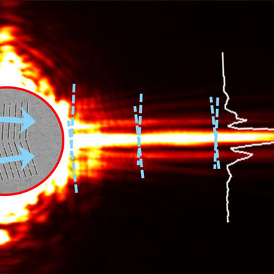 |
| Researchers led by Federico Capasso at SEAS demonstrated a cosine-Gauss plasmon beam, dubbed a "needle beam," that propagates without diffraction. The advance may assist the development of ultrapowerful microprocessors. (Image: Patrice Genevet.)
|
|
The needle beam arises from a special class of quasiparticles called surface plasmons, which travel in tight confinement with a metal surface. The metallic stripes that carry these surface plasmons have the potential to replace standard copper electrical interconnects in microprocessors, enabling ultrafast on-chip communications.
|
|
One of the fundamental problems that has so far hindered the development of such optical interconnects is the fact that all waves naturally spread laterally during propagation, a phenomenon known as diffraction. This reduces the portion of the signal that can actually be detected.
|
|
"We have made a major step toward solving this problem by discovering and experimentally confirming the existence of a previously overlooked solution of Maxwell's equations that govern all light phenomena," says principal investigator Federico Capasso, Robert L. Wallace Professor of Applied Physics and Vinton Hayes Senior Research Fellow in Electrical Engineering at SEAS. "The solution is a highly localized surface plasmon wave that propagates for a long distance, approximately 80 microns in our experiments, in a straight line without any diffraction."
|
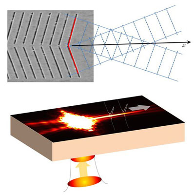 |
| Top: A micrograph and diagram of the metallic gratings that produce the needle beam. Bottom: An approximation of the experimental setup. A laser is focused from the glass substrate side onto the device. Once the non-diffractive surface wave is created, detailed information on its intensity distribution is gathered using an ultrahigh-spatial-resolution near-field scanning optical microscope. (Image: Patrice Genevet.)
|
|
The so-called needle beam, the technical term for which is a cosine-Gauss plasmon beam, propagates in tight confinement with a nanostructured metal surface. Lead author Jiao Lin, a visiting postdoctoral fellow at SEAS from the Singapore Institute of Manufacturing and Technology, and coauthor Patrice Genevet, a research associate in Capasso's group, found an ingenious way to demonstrate the theorized phenomenon. They sculpted two sets of grooves into a gold film that was plated onto the surface of a glass sheet. These tiny grooves intersect at an angle to form a metallic grating. When illuminated by a laser, the device launches two tilted, plane surface waves which interfere constructively to create the non-diffracting beam.
|
|
"Our French colleagues did a beautiful experiment, using an ultrahigh-resolution microscope to image the needle-shaped beam propagating for a long distance across the gold surface," says Genevet.
|
|
Capasso's team hopes the finding will assist the development of more energy-efficient and powerful microprocessors.
|

