| Mar 20, 2014 |
Discovery of new semiconductor holds promise for 2D physics and electronics
|
|
(Nanowerk News) From super-lubricants, to solar cells, to the fledgling technology of valleytronics, there is much to be excited about with the discovery of a unique new two-dimensional semiconductor, rhenium disulfide, by researchers at Berkeley Lab’s Molecular Foundry. Rhenium disulfide, unlike molybdenum disulfide and other dichalcogenides, behaves electronically as if it were a 2D monolayer even as a 3D bulk material. This not only opens the door to 2D electronic applications with a 3D material, it also makes it possible to study 2D physics with easy-to-make 3D crystals.
|
|
“Rhenium disulfide remains a direct-bandgap semiconductor, its photoluminescence intensity increases while its Raman spectrum remains unchanged, even with the addition of increasing numbers of layers,” says Junqiao Wu, a physicist with Berkeley Lab’s Materials Sciences Division who led this discovery. “This makes bulk crystals of rhenium disulfide an ideal platform for probing 2D excitonic and lattice physics, circumventing the challenge of preparing large-area, single-crystal monolayers.”
|
 |
| Nano-beam electron diffraction pattern of rhenium disulfide with a zoom-in insert image reveals a quasi-hexagonal reflection pattern.
|
|
Wu, who is also a professor with the University of California-Berkeley’s Department of Materials Science and Engineering, headed a large international team of collaborators who used the facilities at the Molecular Foundry, a U.S Department of Energy (DOE) national nanoscience center, to prepare and characterize individual monolayers of rhenium disulfide. Through a variety of spectroscopy techniques, they studied these monolayers both as stacked multilayers and as bulk materials. Their study revealed that the uniqueness of rhenium disulfide stems from a disruption in its crystal lattice symmetry called a Peierls distortion.
|
|
“Semiconducting transition metal dichalcogenides consist of monolayers held together by weak forces,” says Sefaattin Tongay, lead author of a paper describing this research in Nature Communications ("Monolayer behaviour in bulk ReS2 due to electronic and vibrational decoupling") for which Wu was the corresponding author. The paper was titled “Monolayer behaviour in bulk ReS2 due to electronic and vibrational decoupling.”
|
|
“Typically the monolayers in a semiconducting transition metal dichalcogenides, such as molybdenum disulfide, are relatively strongly coupled, but isolated monolayers show large changes in electronic structure and lattice vibration energies,” Tongay says. “The result is that in bulk these materials are indirect gap semiconductors and in the monolayer they are direct gap.”
|
|
What Tongay, Wu and their collaborators found in their characterization studies was that rhenium disulfide contains seven valence electrons as opposed to the six valence electrons of molybdenum disulfide and other transition metal dichalcogenides. This extra valence electron prevents strong interlayer coupling between multiple monolayers of rhenium disulfide.
|
|
“The extra electron is eventually shared between two rhenium atoms, which causes the atoms to move closer to one another other, forming quasi-one-dimensional chains within each layer and creating the Peierls distortion in the lattice,” Tongay says. “Once the Peierls distortion takes place, interlayer registry is largely lost, resulting in weak interlayer coupling and monolayer behavior in the bulk.”
|
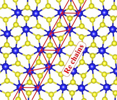 |
| Atomic structure of a monolayer of rhenium disulphide shows the dimerization of the rhenium atoms as a result of the Peierls, forming a rhenium chain denoted by the red zigzag line.
|
|
Rhenium disulfide’s weak interlayer coupling should make this material highly useful in tribology and other low-friction applications. Since rhenium disulfide also exhibits strong interactions between light and matter that are typical of monolayer semiconductors, and since the bulk rhenium disulfide behaves as if it were a monolayer, the new material should also be valuable for solar cell applications. It might also be a less expensive alternative to diamond for valleytronics.
|
|
In valleytronics, the wave quantum number of the electron in a crystalline material is used to encode information. This number is derived from the spin and momentum of an electron moving through a crystal lattice as a wave with energy peaks and valleys. Encoding information when the electrons reside in these minimum energy valleys offers a highly promising potential new route to quantum computing and ultrafast data-processing.
|
|
“Rhenium atoms have a relatively large atomic weight, which means electron spin-orbit interactions are significant,” Tongay says. “This could make rhenium disulfide an ideal material for valleytronics applications.”
|
|
The collaboration is now looking at ways to tune the properties of rhenium disulfide in both monolayer and bulk crystals through engineered defects in the lattice and selective doping. They are also looking to alloy rhenium disulfide with other members of the dichalcogenide family.
|

