| Posted: Nov 22, 2010 |
Toward sub-20 nm hybrid nanofabrication |
| (Nanowerk Spotlight) Lithography is the backbone of the semiconductor industry. Over the past few decades, the microelectronics and data-storage industries have been able to shrink the size of their devices and the size of the patterns that you need to make those devices, following the use of the same types of lithographic materials, tools and strategies, only getting better and better at it. Now, the materials and tools of lithography techniques traditionally used to pattern microelectronics are reaching their fundamental technical limits and researchers have been experimenting with novel materials – for instance self-assembling copolymers – and techniques to extend the reach of today's patterning techniques further downward, i.e. into the sub-20nm range. |
| The workhorse of current nanofabrication processes, electron beam lithography (EBL), has good resolution but it is difficult to precisely control the pattern size at the sub-20 nm scale due to the proximity effect and the large beam spot. A more recent nanolithographic strategy, the molecular ruler (MR) method, shows great promise it can precisely control the size of the gap at the nanoscale. Here, molecular layers of precisely defined widths coat preexisting structures and form templates for patterning nanoscale structures. These gaps can be tailored with molecular scale precision. However, the MR method alone cannot define complex patterns. |
| Although EBL and MR have been combined before in attempting high-resolution nanofabrication in the sub-20nm regime, the results were always less than optimal because the electron beam irradiation damage to the MR influenced the formation of nanogaps. |
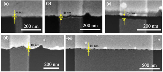 |
| Figure 1: SEM images of nanogaps with different pattern sizes and different gap sizes. (a) 6 nm nanogap with a 60 nm wide daughter pattern; (b) 10 nm nanogap with a 150 nm wide daughter pattern; (c) 20 nm nanogap with a 300 nm wide daughter pattern; (d) 10 nm nanogap with a saw-toothed edge: the nanogap shape is determined by the parent pattern and (e) 10 nm nanogap with a 2 µm wide daughter pattern. (Reprinted with permission from IoP Publishing) |
| Researchers in Japan have now developed a post-EBL process, which does not damage MR molecular layers, and fabricated nanogap structures at the expected positions with high product yield. This novel technique can precisely control the gap size in the sub-20 nm scale by using the MR method to compensate for the resolution limitation of EBL. This method, which gives a well-defined gap size between narrow electrodes with nanoscale width, also enables the measurement of the electrical properties of nanostructures such as nanoparticles and/or single molecules. |
| Reporting their findings in the November 16, 2010 online issue of Nanotechnology ("Toward sub-20 nm hybrid nanofabrication by combining the molecular ruler method and electron beam lithography") a team from the International Center for Materials Nanoarchitectonics at National Institute for Materials Science, and Osaka University, has successfully fabricated a sub-20 nm nanogap device at a desired position by combining the MR method and EBL. |
| A key element in the new technique is a post-EBL self-assembly process that prevents damaging the MR with the high-energy electron beam. This process is shown in the illustration below: |
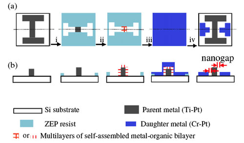 |
| Figure 2: Schematic of the post-EBL process for fabricating nanogap devices. (a) Top view and (b) side view along the dotted line. Process i: define the second pattern on parent metal substrate by EBL and develop in ZED-N50; process ii: self-assemble a few bilayers of molecular resist only at patterned area defined by EBL; process iii: daughter metal evaporation; process iv: lift off in ZDMAC and ACT935J solutions, respectively. (Reprinted with permission from IoP Publishing) |
| Using this method, the Japanese team successfully fabricated high-quality nanogap structures with various sized patterns and gaps in high yield (over 70%). They found that all the edges of EBL patterned structures are straight and it suggests that the developed post-EBL process enables them to control the positions and sizes of the nanogap with full use of the resolutions of EBL and MR. |
| They report that, in their experiments, three, five and ten bilayers of MHDA and Cu2+ ions were self-assembled and the devices exhibited gap sizes of 6 nm, 10 nm and 20 nm, respectively. "It precisely controls the gap size in sub-20 nm scale by combining the MR method to compensate for the resolution limitation of EBL. |
| As shown in (d) in Figure 1, the shape of the nanogap was determined by the parent pattern since the MR was formed just along the edges of the parent patterns. The MR controlled the gap size and the second EBL defined the width of the daughter metal. |
| The researchers also note that their process enabled fabrication of longer nanogap structures with high quality and high yield. |
 By
Michael
Berger
– Michael is author of four books by the Royal Society of Chemistry:
Nano-Society: Pushing the Boundaries of Technology (2009),
Nanotechnology: The Future is Tiny (2016),
Nanoengineering: The Skills and Tools Making Technology Invisible (2019), and
Waste not! How Nanotechnologies Can Increase Efficiencies Throughout Society (2025)
Copyright ©
Nanowerk LLC
By
Michael
Berger
– Michael is author of four books by the Royal Society of Chemistry:
Nano-Society: Pushing the Boundaries of Technology (2009),
Nanotechnology: The Future is Tiny (2016),
Nanoengineering: The Skills and Tools Making Technology Invisible (2019), and
Waste not! How Nanotechnologies Can Increase Efficiencies Throughout Society (2025)
Copyright ©
Nanowerk LLC
|

Become a Spotlight guest author! Join our large and growing group of guest contributors. Have you just published a scientific paper or have other exciting developments to share with the nanotechnology community? Here is how to publish on nanowerk.com. |
