| Posted: Aug 23, 2018 |
Crystalline structure 'a la carte' - Laser-assisted photoactivation of TiO2 films at room temperature and ambient air |
| (Nanowerk Spotlight) Titanium dioxide (TiO2) is a widely used material in applications that include coatings, pharmaceuticals, cosmetics, and photocatalysis – including for water splitting and electricity generation. |
| "All these applications of TiO2 stem from its unique optoelectronic properties, which strongly depend on the crystalline structure," Jaime A. Benavides, a Chemical Engineer, and Ph.D. Candidate in the Research Group in Nano-engineered Optoelectronic Materials & Advanced Devices (NOMAD) at the École de Technologie Supérieure in Montreal, tells Nanowerk. "However, achieving high-quality crystalline TiO2 films at room-temperature remains one of today’s most important technical challenges toward low-cost optoelectronic devices including photovoltaic cells and photocatalytic device architectures." |
| Starting from amorphous TiO2, thermal annealing between 450°C and 1100°C is generally required to achieve the desired crystalline structure for most applications. High-temperature treatment is also generally used to sinter nanocrystalline TiO2 particles and form interconnected nanoparticle networks. |
| Unfortunately, the high temperatures required to manufacture TiO2's anatase and rutile crystalline phases can also be most detrimental to temperature-sensitive devices such as sensors and other optoelectronics. |
| From research to industrial applications, the ability to include thin layers of crystalline TiO2 without involving high temperature or additional chemical processes is a pivotal point to expand the market of this material. |
| In new work, reported in a paper in ACS Applied Energy Materials ("Laser Selective Photoactivation of Amorphous TiO2 Films to Anatase and/or Rutile Crystalline Phases") and first-authored by Benavides, the NOMAD team demonstrates a much simpler method for triggering the crystallization of a TiO2 sol-gel precursor at low-energies. |
| "With our technique, it is now possible to achieve 90% crystallinity without metallic dopants, at room temperature and in ambient air, using low-power laser-induced photoactivation of an amorphous TiO2 nanoparticle film," Benavides points out. "Furthermore, we showed that spatially controlled crystallization of any phase of interest (anatase or rutile) or even a mix of both is easily achieved on amorphous TiO2 films." |
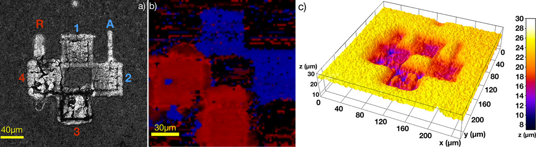 |
| Patterning on-demand crystalline structure. (a) Laser scanning microscope image (LEXT OLS4100; Olympus) of checkered pattern over amorphous TiO2 films. Anatase TiO2 is generated in squares 1 and 2, whereas rutile TiO2 is generated in the squares 3 and 4. (b) Micro-Raman image of the pattern. The blue and red colors represent anatase and rutile TiO2, respectively. (c) Topographic 3D surface reconstructions for the checkered pattern. 3D image generated using software ImageJ based on the data given by the laser scanning microscope analysis. (Reprinted with permission from American Chemical Society) (click on image to enlarge) |
| The key to the researchers' findings lies in the generation and exploitation of surface defects (oxygen vacancies) in nanometric TiO2. |
| With this technique it is possible to have thin-films with anatase and rutile crystalline structure next to each other. The phase transition can be controlled with remarkable precision, reproducibility, and control by using a 532nm laser. |
| This novel process also avoids costly high-temperature, ion-metal-assisted, or specific atmospheric processing that currently prevents the integration of TiO2 in several optoelectronic platforms. |
| Benavides explains that there is a complete understanding on why and how surface defects may alter the properties of materials and more particularly the properties of TiO2. "But the research on TiO2 phase transition exploiting surface defects reported in the body of literature was only done for powders, or using metallic dopants such as Fe or Al or under vacuum conditions or argon atmosphere." |
| The team expects that their work will mainly benefit applications in the areas of energy conversion, energy storage and environmental applications. The level of control and the ability to engineer the TiO2 crystalline structure at the microscopic scale allows the design and fabrication of novel high-performance TiO2 hybrids. They also see flexible printed electronics for solar cells, photodetectors, photocatalytic applications, capacitors and even memristors benefitting from their process. |
| Furthermore, the process presented in the paper is scalable to industrial-scale production environments and it is perfectly compatible with emerging laser-based 3D printing technologies. |
| The team is already working to improve this technology to make it perfectly compatible with laser-based 3D printing and they are developing optoelectronic and photovoltaic devices using this process. |
| They are also looking at opportunities to create a startup to commercialize their patent-pending technology. |
 By
Michael
Berger
– Michael is author of four books by the Royal Society of Chemistry:
Nano-Society: Pushing the Boundaries of Technology (2009),
Nanotechnology: The Future is Tiny (2016),
Nanoengineering: The Skills and Tools Making Technology Invisible (2019), and
Waste not! How Nanotechnologies Can Increase Efficiencies Throughout Society (2025)
Copyright ©
Nanowerk LLC
By
Michael
Berger
– Michael is author of four books by the Royal Society of Chemistry:
Nano-Society: Pushing the Boundaries of Technology (2009),
Nanotechnology: The Future is Tiny (2016),
Nanoengineering: The Skills and Tools Making Technology Invisible (2019), and
Waste not! How Nanotechnologies Can Increase Efficiencies Throughout Society (2025)
Copyright ©
Nanowerk LLC
|

Become a Spotlight guest author! Join our large and growing group of guest contributors. Have you just published a scientific paper or have other exciting developments to share with the nanotechnology community? Here is how to publish on nanowerk.com. |
