Showing Spotlights 1609 - 1616 of 2790 in category All (newest first):
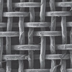 In the last couple of years, there has been particularly growing interest worldwide in exploring ways of finding suitable solutions to clean up oil spills and deal with industrial oily wastewater through use of nanomaterials. Key for the success of these materials is a high separation capacity, with resistance to oil fouling, and that are easily recyclable. Oil/water separation is an interfacial challenge, and novel materials designed to possess special wettability have different interaction and affinity for oil and water, thus can realize the separation. Until now, researches in this field all focus on materials with both hydrophobic and oleophilic properties. However, the oil-removing type of materials is easily fouled even blocked up by oils because of their intrinsic oleophilic property. A novel superhydrophilic and underwater superoleophobic hydrogel coated mesh can selectively separate water from oil/water mixtures effectively and without any extra power.
Sep 1st, 2011
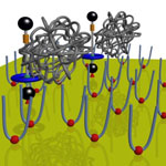
 Most molecular probes used in biomedical research require dyes or fluorescence in order to obtain meaningful signals. These probes usually are quite limited with regard to the complexity of what they can image - be it the measurable concentration range or the number of molecules that can be simultaneously detected. This is an issue that is particularly relevant when it comes to track the simultaneous multiple molecular transformations that dictate complicated diseases like cancer. Scientists now have come up with an intriguing new class of molecular probes to solve this problem. They took an existing spectroscopic technique - surface-enhanced Raman scattering (SERS) - and developed a unique class of nanoparticle labels that provide for different responses when excited by laser light.
Aug 30th, 2011
 Clean and affordable energy generation and storage is one of the most significant challenges that our world is facing in the 21st century. Materials are going to play a crucial role in generation and storage of renewable energy. While searching for new materials for electrical energy storage, materials scientists have discovered a new family of two-dimensional compounds proposed to have unique properties that may lead to ground-breaking advances in energy storage technology. Researchers transformed three dimensional titanium-aluminum carbide into a two dimensional structure with greatly different properties. This work opens the door for a wide range of metal carbide and/or nitride compositions in form of 2-D sheets.
Aug 29th, 2011
 Previously, synthetic molecular machines have been used to perform mechanical tasks collectively, such as move liquid droplets uphill against the force of gravity, rotate microscale objects using liquid crystals doped with synthetic motor-molecules, and bend cantilevers. However, all these tasks are achieved by the collective action of billions and billions of molecular machines. Observing the mechanical behavior of an individual molecule is much more difficult. Synthetic molecular machines are often ten times smaller in each dimension than motor proteins and previously no one has managed to use single molecule techniques to look at how the components move in synthetic molecular machines. By using very sensitive atomic force microscopy experiments, researchers now were able to address the movement of the ring in individual rotaxane molecules.
Aug 26th, 2011
 It is quite difficult - not least because there is no consensus about a proper definition - to assess the scope of nanotechnology research and its impact on the overall scientific body as well as its commercialization prospects. In a new attempt to put some numbers behind the general perception of a rapidly expanding nanotechnology field, two researchers at UC Davis have trawled scientific databases and come up with some surprising findings. For instance, that China has now overtaken the USA in annual research paper output related to nanoscience and nanotechnology. Also, the proportion of "nano"-related articles relative to the total size of the subject categories (such as physics, materials sciences or chemistry) has risen dramatically over the past 13 years.
Aug 23rd, 2011
 Electronic devices with muscles-like stretchability have long been pursued, but not achieved due to the requirement that all materials in the devices - electrodes, semiconductor, and dielectric - are stretchable. In their pursuit of fully flexible and stretchable electronic devices, researchers have already reported stretchable solar cells and transistors as well as stretchable active-matrix displays. The nanomaterials used for these purposes range from coiled nanowires to graphene. Recently, researchers at UCLA have successfully demonstrated a stretchable polymer composite that is highly transparent and highly conductive, and applied this nanocomposite material to fabricating stretchable devices. This work represents a proof-of-concept, highly stretchable semiconductor device wherein every part of the device is intrinsically stretchable.
Aug 22nd, 2011
 Molecular separations are extremely important in a wide range of technologies, from conventional proteomics to pathogen detection and DNA fingerprinting. A complication arises from the fact that molecular components in mixtures can span an enormous range of concentration. Conventional approaches such as antibody depletion are not sensitive enough to detect numerous medically significant biomarkers, whose incidence in blood could be as much as a trillion times less abundant than the most plentiful protein, albumin. New research shows a new path in miniaturized molecular separations. It describes a new device that demonstrates simultaneous concentration and separation of proteins by conductivity gradient focusing. Concentration and separation take place in an electric-field-driven 120 nm deep nanochannel that supports a stable salt and conductivity gradient. The results show that relevant proteins can be concentrated to detectable levels.
Aug 18th, 2011
 The atomic structures of nanoscale contacts are not available in most experiments on quantum transport. Scanning tunneling microscopy operates at a tip-sample distance of a few angstroms and relies on probing a conductive surface in the evanescent tail of electronic states. By decreasing the tip-sample distance the sensitivity to chemical interactions can be enhanced. This has already been demonstrated in non-contact atomic force microscopy, where the oscillating tip comes for short periods of time within the range of chemical interactions. A team of scientists has now developed Quantum Point Contact Microscopy as a novel imaging mode of low-temperature STM, where instead of measuring a current through a tunneling junction, a transport current through a quantum point contact formed by a single atom between the STM tip and the surface is recorded.
Aug 16th, 2011
 Subscribe to our Nanotechnology Spotlight feed