Showing Spotlights 777 - 784 of 2786 in category All (newest first):
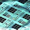 Perovskite materials have attracted great attention in the fields of optoelectronics due to their significant optoelectronic properties. So far, the applications of perovskite thin-films have been limited to solar cells because the required high-definition patterning for optoelectronic devices hadn't been achieved yet. Now, though, researchers in Korea have realized a high-resolution spin-on-patterning (SoP) process for the fabrication of optoelectronic devices arrays such as image sensors.
Sep 5th, 2017
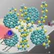
 The implantation of orthopaedic devices is associated with a high risk of post-operative complications that increases substantially with each revision surgery. Researchers now have proposed a two-pronged strategy to address this outstanding clinical problem by combatting infections and providing bioactivity for titanium implants. Their nanostructured surfaces simultaneously are highly antimicrobial as well as bioactive - the goal of combining both functions without inducing cytotoxicity has thus far proved elusive.
Sep 4th, 2017
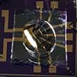
 Photothermal induced resonance (PTIR) has found application in the characterization of materials in fields spanning from photovoltaics, plasmonic, polymer science, biology and geology to name a few. PTIR combines the spatial resolution of atomic force microscopy with the specificity of absorption spectroscopy, enabling mapping of composition and electronic bandgap, material identification and biomolecule conformational analysis with nanoscale spatial resolution. Scientists have now implemented, for the first time, an integrated near-field cavity-optomechanics readout concept to realize fully functional nanoscale AFM probes capable of ultralow detection noise within an extremely wide measurement bandwidth in ambient conditions, surpassing all previous AFM probes.
Sep 1st, 2017
 Molecular ferroelectrics are highly desirable as they are environmentally friendly, light-weight, and high spontaneous polarized. Though intensive studies have been focused on molecular ferroelectrics, very few researchers have tried to address the issue of thin film growth. An international research team now presents the first report on the preparation of high-quality large area MOFE films using in-plane liquid phase growth. With this approach, different kinds of novel ferroelectric films can be grown for potential practical applications such as temperature sensing, data storage, actuation, energy harvesting and storage.
Aug 31st, 2017
 Current insulin detection methods are time-consuming with a low sensitivity, and are hence not adequate for rapid and direct detection of insulin at clinically appropriate concentrations. A novel graphene nanotechnology sensor is highly sensitive to changes in the charge distribution on and in the immediate vicinity of the graphene surface and can respond to physiological insulin concentration variations in a sensitive and rapid manner, thereby enabling real-time insulin monitoring.
Aug 30th, 2017
 New work work shows the state of the art of engineering in wearable display technology. Researchers have demonstrated a passive matrix quantum dot light-emitting diode (QLED) display fully integrated with flexible electronics. They realized the visualization of meaningful information such as images, recorded healthcare data, and other messages using their display. This ultrathin and ultrasoft QLED array can be conformally laminated on human skin.
Aug 29th, 2017
 Due to their unique interlayer coupling and optoelectronic properties, van der Waals heterostructures are of considerable interest for the next generation nanoelectronics. Conventional 2D heterostructures usually are composed of two layers of opposite charge carrier type using inorganic materials. One of the challenges when creating 2D heterostructures is the painstaking stacking of the individual components on top of each other. Researchers have now found, for the first time, that there can also be charge transfer (CT) induced interfacial coupling between two different pairs of organic CT layers.
Aug 23rd, 2017
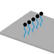 Synthetic nanomotors and DNA walkers, which mimic a cell's transportation system, are intricately designed systems that draw chemical energy from the environment and convert it into mechanical motion. Using such DNA walkers as signal amplifier for nucleic acids detection has only recently been reported. Researchers now report that they converted a DNA walker into a linear fluorescence signal amplifier on a rectangle DNA origami that can improve the detection of target molecules such as nucleic acids.
Aug 21st, 2017
 Subscribe to our Nanotechnology Spotlight feed