| Posted: Oct 01, 2009 | |
Nanotechnology electronics at the tip of your gloved finger |
|
| (Nanowerk Spotlight) Imagine this: Chip-based credit cards and other smart cards on paper; intelligent sensors and electronics on doctors' surgical gloves; health monitors printed on T-shirts; diagnostic devices embedded in your baby's diapers; human machine interfaces on workers' leather gloves. These are just some of the systems that researchers envision today and that will become reality tomorrow thanks to research teams like John Rogers' group at the University of Illinois. | |
| Nanotechnology-enabled electronics of the future will be invisible, i.e. transparent (see "Invisible electronics made with carbon nanotubes"), or flexible, or both. One of the areas Rogers' group focus on is creating materials and processes that will allow high-performance electronics that are flexible and stretchable (see our previous Spotlight "Gutenberg + nanotechnology = printable electronics"). | |
 |
|
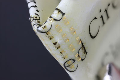
| Electronic circuit on folded paper. (Image: Rogers group, University of Illinois) | |
| Previous work by Rogers' group showed the ability to use silicon nanomaterials for flexible and stretchable circuits on plastic and rubber substrates, respectively. In their recent work, they build on those strategies and extend them for other classes of substrate, by incorporating thin, low modulus layers between the circuits and the substrates to isolate, to a useful and important degree, the circuits from strains induced in the substrate by folding, bending, stretching or any other complex or simple mode of deformation. | |
| "We have demonstrated examples of CMOS circuits on paper, fabric, leather and vinyl," Rogers tells Nanowerk. "To our knowledge, this is the first example of active electronics integrated with such substrates. An additional advantage of our approaches is that the properties of the circuits and transistors are as good as those of devices with comparable feature sizes formed on the rigid, brittle surfaces of semiconductor wafers. The use of silicon as the active material enables this outcome." | |
| Reporting their findings in a recent issue of Advanced Materials ("Ultrathin Silicon Circuits With Strain-Isolation Layers and Mesh Layouts for High-Performance Electronics on Fabric, Vinyl, Leather, and Paper"), Rogers' group has now demonstrated that the combined use of circuits with non-coplanar serpentine mesh designs and thin, low modulus strain isolation layers allows integration of high performance silicon CMOS integrated circuits on diverse substrates. | |
| The researchers start their fabrication process with the formation of ultrathin CMOS circuits in planar, serpentine mesh geometries using procedures closely related to what they had reported recently ("Materials and noncoplanar mesh designs for integrated circuits with linear elastic responses to extreme mechanical deformations"). After lifting the circuits from the carrier wafer and depositing them on a silicon-based organic polymer (PDMS) stamp, they coat the backside of the active circuit regions with a 3-30 nm thick chromium/silicon dioxide bilayer and then through transfer print the circuit onto a substrate coated with a thin layer of cured PDMS. | |
| "This thin layer of PDMS serves two critically important roles," explains Rogers. "First, and most simply, it provides an adhesive that bonds certain strategic regions of the circuits to a wide range of surfaces including fabric, vinyl, leather and paper – in either flat or curved, balloon-like shapes. Secondly, it provides tensile strain isolation in cases where the underlying material is stretched, compressed or bent." | |
 |
|
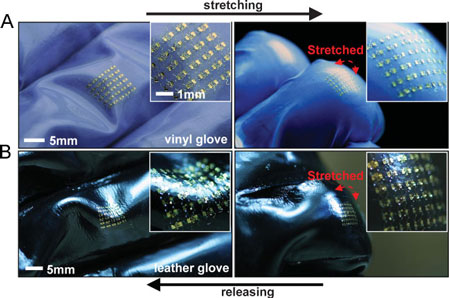
| Optical images of CMOS circuits on finger joints of vinyl (A) and leather (B) gloves in released (left) and stretched (right) states. The insets provide magnified views. (Reprinted with permission from Wiley-VCH) | |
| To demonstrate their CMOS circuits on leather and vinyl, the team integrated arrays of inverters at finger joints in gloves made of these materials. Moving the fingers causes the circuits to stretch and release, with no noticeable change in the electronic properties. | |
| "Similar circuits on paper are particularly interesting, not only for applications in smart cards and related but also for their capacity to add functionality to paper-based microfluidic diagnostic devices" says Rogers. "This approach to electronics on paper provides an alternative to those that rely on direct thin film deposition of organic or inorganic electronic materials." | |
| At the moment, the team is working toward demonstrators of the types of applications listed above. According to Rogers, latex is an excellent substrate for various biomedical device applications. "Engineering aspects of achieving such systems are topics of current work." | |
 By
Michael
Berger
– Michael is author of three books by the Royal Society of Chemistry:
Nano-Society: Pushing the Boundaries of Technology,
Nanotechnology: The Future is Tiny, and
Nanoengineering: The Skills and Tools Making Technology Invisible
Copyright ©
Nanowerk LLC
By
Michael
Berger
– Michael is author of three books by the Royal Society of Chemistry:
Nano-Society: Pushing the Boundaries of Technology,
Nanotechnology: The Future is Tiny, and
Nanoengineering: The Skills and Tools Making Technology Invisible
Copyright ©
Nanowerk LLC
|
|
|
Become a Spotlight guest author! Join our large and growing group of guest contributors. Have you just published a scientific paper or have other exciting developments to share with the nanotechnology community? Here is how to publish on nanowerk.com. |
|