| Posted: Apr 30, 2007 | |
Electronics can be so transparent |
|
| (Nanowerk Spotlight) One of the newly emerging areas of semiconductor technology is the field of transparent electronics. These thin-film materials hold the promise of a new class of flexible and transparent electronic components that would be more environmentally benign than current electronics. Being able to print transparent circuits on low-cost, flexible, plastic substrates opens up the possibility of a wide range of new applications, ranging from windshield displays and flexible solar cells to clear toys and artificial skins and even sensor implants. It is likely that such flexible see-through structures will find wide uses in military, biosensing and consumer goods due to the advantages of high transparency and reliable electrical characteristics. However, the emerging transparent electronics technology is facing manufacturing problems: current fabricating processes do not separate the device manufacturing from material synthesis. The transparent electronic materials, which are largely inorganic oxides. are directly deposited on the device substrate under harsh conditions which may cause damage to the existing layer or flexible substrate. The etching of small dimension oxide multilayer is also difficult due to the low selectivity of the etching recipe. New research results demonstrate that nanofabrication techniques could solve these problems. | |
| Only a few days ago we reported on a superlattice nanowire pattern transfer (SNAP) approach developed by MIT researchers that could be used to fabricate flexible field-effect transistors ("High performance electronics and sensors on flexible plastic chips"). Now, a group of researchers from Clarkson University and Pacific Northwest National Laboratory report that clear nanocrystals can serve as the appropriate electronic materials in the transparent device. | |
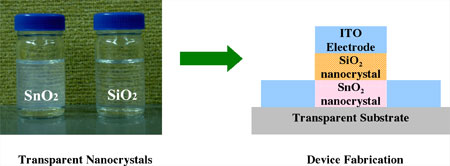
| "The purpose of our work is to demonstrate the fabrication of transparent devices using nanofabrication and nanomaterials" Dr. Feng Hua tells to Nanowerk. "Clear but functional multilayers can be formed with different types of optically transparent nanocrystals via the layer-by-layer (LBL) self-assembly. Our process generates the patterns of the multilayer only using lift-off, thus circumventing the etch-back process." | |
| Hua, an assistant professor in the Electrical & Computer Engineering Department at Clarkson University, goes on to explain that their technique physically separates the synthesis of the transparent nanomaterials from the subsequent transfer onto the substrate, which occurs under mild condition such as room temperature. As a result, the harsh conditions associated with the material synthesis, such as high temperatures, are separated from the device fabrication. The employed bottom-up approach also circumvents the etching of oxide multilayer, which may damage the underlying oxide layers due to the low selectively of the etching process to multiple oxide layers. | |
 |
|
| Schematic showing that the synthesis of the transparent nanomaterials are separated from the device fabrication. The nanomaterials are transferred onto the device substrate after the synthesis. (Image: Dr. Hua) | |
| "Our process shares the merits of LbL assembly such as low cost, simplicity, well-controlled molecular order and room temperature process" says Qiaohui Zhang, a PhD student in Hua's group who did most of the lab work. "As a result, a more clear structure over a large area is allowed." | |
| In addition, the process is composed of many identical dipping steps, which can be readily performed by a programmable robot, allowing for batch and low cost production. | |
| The LbL self-assembled nanocrystal thin-films show a high uniformity which would allow the fabrication of large area devices. Furthermore, this process is applicable to the fabrication of other transparent semiconductor or optoelectronic devices. Other clear nanocrystals can also be used to form the functional layers in the devices. The additive transparent thin films can be coated on almost any material. | |
| Hua says that the success of their work paves the way to future research of integrating high mobility nanowires into transparent circuits. "Our group is already working on transparent sensors and heterogeneous CMOS circuits" he says. | |
| This work, titled "Transparent thin-film transistor with self-assembled nanocrystals", was published in the April 17, 2007 edition of Nanotechnology. | |
 By
Michael
Berger
– Michael is author of three books by the Royal Society of Chemistry:
Nano-Society: Pushing the Boundaries of Technology,
Nanotechnology: The Future is Tiny, and
Nanoengineering: The Skills and Tools Making Technology Invisible
Copyright ©
Nanowerk LLC
By
Michael
Berger
– Michael is author of three books by the Royal Society of Chemistry:
Nano-Society: Pushing the Boundaries of Technology,
Nanotechnology: The Future is Tiny, and
Nanoengineering: The Skills and Tools Making Technology Invisible
Copyright ©
Nanowerk LLC
|
Become a Spotlight guest author! Join our large and growing group of guest contributors. Have you just published a scientific paper or have other exciting developments to share with the nanotechnology community? Here is how to publish on nanowerk.com.