| Posted: Mar 11, 2014 | |
Flexible silicon-on-polymer sub-20 nm FinFETs without performance loss |
|
| (Nanowerk Spotlight) Flexible electronics is a rising field in terms of research and potential application opportunities to obtain similar characteristics than today's prevailing rigid electronics components. In new work, researchers have demonstrated the semiconductor industry’s most advanced device architecture – FinFET, a new generation of device architecture which Intel has adopted in 2011 in their microprocessors; these field effect transistors offer non-planar three-dimensional topology where the channels are vertically aligned in arrays of ultra-thin silicon fins bordered by multiple gates – in a flexible platform using only industry standard processes and keeping the advantages offered by silicon. | |
| Although there are promising developments in the fabrication of flexible electronics using carbon nanotubes and graphene, the electrical superiority achieved with inorganic semiconducting substrates and the maturity of the silicon microfabrication industry make the integration of silicon on flexible platforms a logical next step towards achieving high computational capabilities in mobile devices. This basically means transforming rigid electronic components into flexible ones while keeping their performance. | |
| "Our results show outstanding flexibility and electrical performance, providing a step forward towards very large integration of high performance flexible devices," Muhammad Mustafa Hussain, an Associate Professor of Electrical Engineering at King Abdullah University of Science and Technology (KAUST) in Saudi Arabia, tells Nanowerk. "The most intriguing scientific exploration is how the devices behave in an ultra-thin fully flexible silicon wafer." | |
| Reporting their finding in the February 22, 2014, online edition of Advanced Materials ("Flexible and Transparent Silicon-on-Polymer Based Sub-20 nm Non-planar 3D FinFET for Brain-Architecture Inspired Computation"), the team demonstrates a pragmatic approach to transforming silicon-on-insulator (SOI) based state-of-the-art FinFET into flexible and semi-transparent silicon-on-polymer FinFET while retaining high performance and integration density. | |
 |
|
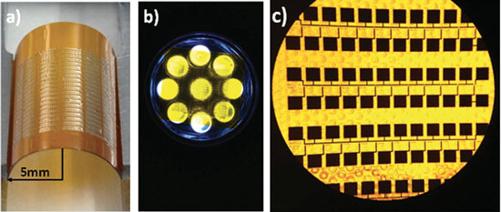
| a) FinFET silicon fabric at minimum device scale bending radius (5 mm). b) Transparency through the flexible silicon with devices, placed on top of a torch. It is to be noted that the fabric is not rolling back rather staying as it is placed without any adhesive or force. c) Optical microscopic image of released devices. (Reprinted with permission from Wiley-VCH Verlag) | |
| This is the first time that 3D architectures on a flexible silicon-based platform are obtained from standard silicon on insulator wafers. At the same time, the researchers are showing a process that is completely industry compatible and does not need additional expensive materials or processes. | |
| "For the past four years, we have been conducting research in the area of flexible electronics and our ultimate goal is the demonstration of consumer electronic products using our flexible platform," says Galo A. Torres Sevilla, a member of Hussain's group and the paper's first author. "With this goal in mind, our research is motivated by our desire to introduce a new concept of high-performance flexible electronics that make use of silicon as their main material." | |
| When fabricating flexible inorganic electronics derived from rigid substrates, many different factors come into play. For example, when bending a device, some electrical characteristics change along with the bending radii. Therefore, in order to create circuitry using these flexible devices, factors such as threshold shift and drive current change have to be taken into account during the design process. | |
| Torres Sevilla points out that the process developed by his team has the unique characteristic that all the devices can be fabricated prior to release without any constraint set by the high thermal budget or by the etch holes due to the extremely high etch selectivity between silicon and silicon dioxide. "Our process thus sets a major step towards the integration of state-of-the-art high performance devices for ultra-mobile brain-inspired foldable computers or ICs." | |
| The specific steps of the team's FinFET P- and N- MOS fabrication process has been described in previous work ("Gate-First Integration of Tunable Work Function Metal Gates of Different Thicknesses Into High-κ /Metal Gates CMOS FinFETs for Multi-VTH Engineering "). | |
| "We have chosen to demonstrate high performance P- and N- MOS devices in flexible silicon fabric (in a previous Nanowerk Spotlight we reported on the team's work on flexible and semitransparent silicon electronics) to prove the compatibility of our process with the backbone of high performance CMOS based electronics," says Hussain. "Although we have not shown complete circuitry on flexible silicon fabric due to mismatched VTH shift in P-MOS devices, this work indicates that with the correct process optimization and integration of dual high-κ/metal gate for threshold voltage correction, we can transform large scale state-of-the-art high performance circuitry without affecting its performance." | |
| According to the researchers, electrical characterization of the devices shows a sub-threshold swing of 80 mVdec-1 for NMOS and 70 mVdec-1for PMOS and Ion/Ioff ratio of 4.6 decades for NMOS and 4.78 decades for PMOS. | |
| Hussain points out that, since the fabric is extremely thin and the host substrate is a polyimide sheet, the complete set of devices exhibits semitransparency. | |
| The vision and research goal of Hussain's group is to ensure smart interactive electronics which are fully flexible – every single component of a complex electronic system will be flexible and thus portable and massively deployable. This present work is a big step in that direction. | |
 By
Michael
Berger
– Michael is author of three books by the Royal Society of Chemistry:
Nano-Society: Pushing the Boundaries of Technology,
Nanotechnology: The Future is Tiny, and
Nanoengineering: The Skills and Tools Making Technology Invisible
Copyright ©
Nanowerk LLC
By
Michael
Berger
– Michael is author of three books by the Royal Society of Chemistry:
Nano-Society: Pushing the Boundaries of Technology,
Nanotechnology: The Future is Tiny, and
Nanoengineering: The Skills and Tools Making Technology Invisible
Copyright ©
Nanowerk LLC
|
|
|
Become a Spotlight guest author! Join our large and growing group of guest contributors. Have you just published a scientific paper or have other exciting developments to share with the nanotechnology community? Here is how to publish on nanowerk.com. |
|