| Posted: Mar 07, 2008 | |
Nanotechnology grinders |
|
| (Nanowerk Spotlight) 'Field evaporation' is the phenomenon by which surface atoms are ionized (evaporated) under an applied, extremely high electric field of the order of several volts per nanometer. Electric fields of this magnitude can only be achieved by applying a high field to an extremely sharp needle such as the specimen tip in a Field Ion Microscope. Field evaporation was first reported over 50 years ago and has since developed into the powerful Atom Probe Field Ion Microscopy which is able to reproduce the atomic structure of a piece of material in three dimensions. | |
| Today, field evaporation is mainly used for material characterization, and the behavior of nanomaterials at extremely strong electric fields is of great scientific and technological interest. In principle, the field evaporation phenomenon can be utilized not only for materials characterization, but also for materials processing and morphology control with extremely high precision because of its unique atom-by-atom removal capability. However, detailed structural evolution of nanomaterials during field evaporation has never been directly observed and this limitation has greatly restricted the potential applications of field evaporation as a materials-processing tool. | |
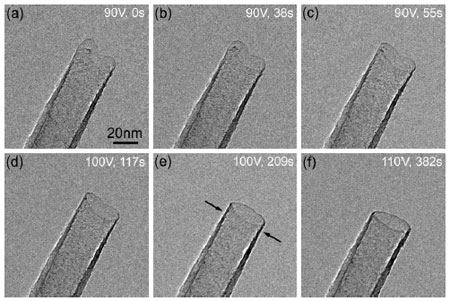
| Now, researchers in Beijing have reported the first direct observation of field evaporation phenomena using a transmission electron microscopy (TEM) technique. By conducting in situ TEM field evaporation experiments on individual carbon nanotubes (CNTs), the researchers were able to reveal details about the structural evolution of the nanomaterials via direct observation. Using this technique, they have been able to perform controlled engineering of the CNTs with atomic precision, for example, grinding and shortening of CNTs, shaping of the open ends of CNTs, and opening of CNT caps. | |
| "In traditional Field Ion Microscopy and atom probe investigation, the field evaporation phenomenon is mainly utilized for material characterization, and only the structural information on the tip surface or the evaporated segments of the specimen can be obtained, instead of “seeing” the structural evolution of the sample directly" Dr. Lian-Mao Peng explains to Nanowerk. "Our work provides the first direct observation of the detailed structural evolution of nanomaterials during field evaporation. We also show that field evaporation can be utilized not only for material characterization, but also for material processing and morphology control with extremely high precision." | |
| Peng is director of the Key Laboratory for the Physics and Chemistry of Nanodevices and professor of Nanoscale Science and Technology at Peking University. In a new paper published in the January 29, 2008 online edition of Advanced Materials, Peng and his group demonstrate that positive field evaporation in combination with in situ TEM may actually provide a very simple and effective means for controlling the morphology of nanomaterials with atomic precision ("Grinding a Nanotube"). | |
| Peng notes that – analogous to laser-stimulated field evaporation – an electron beam has a similar effect for promoting the field emission process. However, the size of the laser beam is typically several micrometers and covers the entire area of the probed nanomaterial. In contrast, the spot size of the electron beam in a TEM can be made as small as few or even sub-nanometer. "The desired sample area may therefore be selected by the electron beam conveniently and precisely, and site-selective evaporation may be promoted" he says. | |
 |
|
| Evolution of the end structure of a CNT during field evaporation. The series of TEM images record the end smoothening and shortening process. The arrows in (e) indicate the final CNT termination site in (f). (Reprinted with permission from Wiley-VCH Verlag) | |
| He also points out that many other approaches have been developed to control the length or end structure of individual CNTs, for example, the cutting of CNTs by various methods such as the use of an AFM tip, a focused e-beam, a CNT 'nanoknife' (also developed be Peng's group), and electron ablation have been reported. | |
| "Compared to these methods, which have a precision of only several to several tens of nanometers, the most notable advantage of our in situ field evaporation method is the extremely high precision in controlling the CNT length" explains Peng. "On average, over a period of several seconds (or even longer), only one layer of carbon atoms is evaporated from the end of a CNT. Furthermore, positive field evaporation is a self-regulating process wherein the emitter surface can be processed to become very regular in shape and smooth at the atomic scale. Owing to these two advantages of our method, we believe that we have achieved atomic precision, which is hardly achievable by other approaches." | |
| Field evaporation depends critically on the local electric field, which means that the atoms subjected to the highest local electric field are the first to be evaporated. Consequently, in most cases, once the initial end structure is obtained, the subsequent evolution of this end structure towards the final end structure is basically predetermined. "Usually all we can do is to change the speed of evolution or to stop the evaporation at some intermediate but not entirely stable morphology before a steady state is established" says Peng. "In our experiments, we show that in situ TEM field evaporation has the unique capability of changing the evaporation sequence. Therefore, this process enables more precise control of the end structure of nanomaterials." | |
| The Chinese scientists emphasize that their findings show that, in principle, the field evaporation phenomenon can be utilized not only for materials characterization, but also for materials processing and morphology control with extremely high precision. | |
| This unique atom-by-atom removal capability, which may have the potential to replace other existing morphology-control method, could provide highly controlled engineering of nanomaterials. | |
| For example, Peng's group demonstrated that the length of a nanomaterial can be controlled with atomic precision, and its end can be 'ground' to become an atomically smooth structure. The control of length and end structure is very important for improving the performance of single nanomaterials as e.g. field emitter or scanning probe. For instance, the researchers propose that if a vertically aligned CNT film is processed by positive field evaporation, the field emission sites can be made more uniform, resulting in a higher current density and better emission stability, which is highly required for field emission display application. | |
| Another example is opening the caps of CNTs, which is of great importance for nanotechnology: the hollow cores of CNTs can be filled with fullerenes and metal nanowires, thereby forming nanocomposites exhibiting novel electrical and magnetic properties. A crucial step involved in these filling procedures is the opening of the CNT caps by chemical or physical methods. CNTs also have been demonstrated to make nanopipes or nanopipettes in nanofluidic devices, where an open end is required for jetting and imbibing liquids. | |
| "As we have demonstrated, our method not only enables CNTs to be opened, but also provides precise control over the size of the hole in the cap, which may affect the jetting or imbibing rate" says Peng. | |
| In previous work, the team already has demonstrated the controlled removal of carbon atoms at the tip of a CNT and the fabrication of various tip structures (Engineering the cap structure of individual carbon nanotubes and corresponding electron field emission characteristics). This, however, was achieved via electron field emission induced evaporation, instead of field evaporation. Electron field emission is much harder to control than the new technique, resulting in a much less perfect structure. | |
| Peng and his team are now working on getting more higher resolution structural information of the very end tips of nanomaterials, and to observe how a single atom, or cluster of atoms, moves along and away from the surface at the application of an extremely strong field. | |
 By
Michael
Berger
– Michael is author of three books by the Royal Society of Chemistry:
Nano-Society: Pushing the Boundaries of Technology,
Nanotechnology: The Future is Tiny, and
Nanoengineering: The Skills and Tools Making Technology Invisible
Copyright ©
Nanowerk LLC
By
Michael
Berger
– Michael is author of three books by the Royal Society of Chemistry:
Nano-Society: Pushing the Boundaries of Technology,
Nanotechnology: The Future is Tiny, and
Nanoengineering: The Skills and Tools Making Technology Invisible
Copyright ©
Nanowerk LLC
|
Become a Spotlight guest author! Join our large and growing group of guest contributors. Have you just published a scientific paper or have other exciting developments to share with the nanotechnology community? Here is how to publish on nanowerk.com.