Nanotechnology News – Latest Headlines
Researchers devise tunable conducting edge
Physicists demonstrated a new magnetized state in a monolayer of tungsten ditelluride. Called a magnetized or ferromagnetic quantum spin Hall insulator, this material of one-atom thickness has an insulating interior but a conducting edge, which has important implications for controlling electron flow in nanodevices.
September 7, 2022 Read more

Light accelerates conductivity in nature's 'electric grid'
The natural world possesses its own intrinsic electrical grid composed of a global web of tiny bacteria-generated nanowires in the soil and oceans that 'breathe' by exhaling excess electrons.
September 7, 2022 Read more
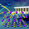
MXene-based biosensor for early cancer detection
This composite membrane utilized the characteristics of large-scale preparation and MXene membrane reducibility, allowing the biosensor to realize good accuracy and stability in exosome determination.
September 5, 2022 Read more

Novel 'nano killers' for sterilization and antifouling
Researchers have found that a MoS2 nanosheets-based vacancy materials activated by permonosulfate enables efficient anaerobic microorganisms disinfection.
September 5, 2022 Read more

Coupling of electron-hole pairs
Researchers have coupled two types of electron-hole pairs - interlayer and intralayer pairs - by bringing the two of them to similar energies. They can therefore tailor-make merged particles that are not only very bright but also interact very strongly with one another.
September 5, 2022 Read more

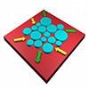
Super-dense packing of hydrogen molecules on a surface
Scientists describe the formation of a superdense monolayer of hydrogen on highly ordered mesoporous silica near the boiling temperature.
September 5, 2022 Read more
Organic thin-film sensors for light-source analysis and anti-counterfeiting applications
A team of physicists and chemists presents an organic thin-film sensor that describes a completely new way of identifying the wavelength of light and achieves a spectral resolution below one nanometer.
September 5, 2022 Read more

A memristive forming strategy for lowering the contact resistances of two-dimensional semiconductors
Two-dimensional (2D) semiconductors, like transition-metal dichalcogenides, have become a competitive alternative to traditional semiconducting materials in the post-Moore era, and caused worldwide interest. However, before they can be used in practical applications, some key obstacles must be resolved. One of them is the large electrical contact resistances at the metal-semiconductor interfaces. Researchers have proposed a brand-new contact resistance lowering strategy of 2D semiconductors with a good feasibility, a wide generality and a high stability.
September 5, 2022 Read more
Combing light with sharper teeth
New research provides a deeper understanding of how the line width in microcombs works, something that will, among other things, enable even more precise measurements in the future.
September 5, 2022 Read more

Multilayer stack opens door to low-power electronics
Researchers found that a stack of ultrathin materials exhibits a phenomenon called negative capacitance, which reduces the voltage required for transistor operation.
September 3, 2022 Read more
Uncovering the atomic mechanism underpinning heat transport in thermoelectric materials
Neutrons reveal remarkable atomic behavior in thermoelectric materials for more efficient conversion of heat into electricity.
September 3, 2022 Read more

New study confirms 'rippled sheet' protein structure predicted in 1953
Scientists report three crystal structures of periodic rippled beta sheets, a novel protein structure with potential applications in biomedicine and materials science.
September 2, 2022 Read more
Physicists develop a linear response theory for open systems having exceptional points
An international team of physicists recently presented a systematic analysis of the linear response of non-Hermitian systems having exceptional points.
September 2, 2022 Read more
Team measures electronic noise more precisely than ever before
Method used could significantly improve how electronic components are tested.
September 2, 2022 Read more

Quantum materials: entanglement of many atoms discovered for the first time
Scientists have discovered an entirely new type of phase transitions. They display the phenomenon of quantum entanglement involving many atoms, which previously has only been observed in the realm of few atoms.
September 2, 2022 Read more

Van der Waals infrared photodetectors based on 'optical' and 'electrical' combined manipulations
Blackbody response is highly desired in two-dimensional (2D) infrared photodetectors, which determines their practical applications. However, limited by the thickness and complex defects of 2D materials, 2D photodetectors still suffer from problems such as low quantum efficiency and large dark current. Researchers now demonstrate fully depleted self-aligned van der Waals (vdW) photodetectors based on a heterosandwiched structure.
September 2, 2022 Read more
 Subscribe to our Nanotechnology News feed