Showing Spotlights 9 - 16 of 44 in category All (newest first):
 Perovskite QLEDs possess the features of wide gamut and real color expression; that's why they have been considered as very promising candidates for next-generation high-quality lighting and displays. However, device efficiency and stability of perovskite QLEDs has always been a major challenge. Researchers now report a new passivation technique that greatly enhances device performance and stability compared to single interface processing.
Aug 10th, 2020
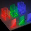 Researchers have fabricated nanoscale color pixels that utilize three-dimensional space to improve and control the brightness of individual pixels with nanoscale lateral dimensions. Specifically, this novel method utilizes 3D printing of vertically freestanding nanostructures containing red, green, or blue light-emitting quantum dots embedded in polymer nanowires. The emission brightness of the pixels linearly increases with the height of the pixels due to the increase in the number of quantum dots due to the increased volume. The 3D geometry enables a 2-fold increase in brightness without causing significant changes in the lateral dimensions of the pixel.
Aug 5th, 2020
 In recent years, black-phosphorus-analogue (BPA) two-dimensional materials have been demonstrated to exhibit promising optoelectronic performances and distinguished ambient stabilities, holding great promise in practical applications. In new work, researchers demonstrated that ultra-small 2D beta-lead oxide quantum dots showed fast carrier dynamics and significantly high photocurrent density and excellent ambient stability. These findings hold great potential for high-performance BPA-based optoelectronic devices.
Nov 6th, 2018
 New work work shows the state of the art of engineering in wearable display technology. Researchers have demonstrated a passive matrix quantum dot light-emitting diode (QLED) display fully integrated with flexible electronics. They realized the visualization of meaningful information such as images, recorded healthcare data, and other messages using their display. This ultrathin and ultrasoft QLED array can be conformally laminated on human skin.
Aug 29th, 2017
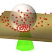 The use of quantum dots (QDs) in practical applications relies on the ability to precisely pattern QDs on substrates with desired optical properties. Typical direct-write printing techniques such as inkjet and gravure printing are limited in resolution (micron-scale), structural complexity, and require significant post-processing time. In new work, researchers use laser-induced bubble printing to pattern CdSe/CdS QDs on plasmonic substrates with submicron resolution, high throughput, and strong QD-substrate adhesion.
May 11th, 2017
 Luminescent quantum dots (LQDs), which possess high photoluminescence quantum yields, flexible emission color controlling, and solution processibility, are promising for applications in lighting systems (warm white light without UV and infrared irradiation) and high quality displays. However, the commercialization of LQDs has been held back by the prohibitively high cost of their production. In a breakthrough approach, researchers have now succeeded in preparing highly emissive inorganic perovskite quantum dots at room temperature.
Mar 7th, 2016
 Ever since the first cadmium selenide quantum dot-based light-emitting devices (QLEDs) were reported in 1994, the dominant materials for QLEDs investigated since then have been limited to wurtzite or zinc blende Cd-based QDs. Similarly, the best developed and studied colloidal QD lasers have been fabricated from Cd-based semiconductors. Now, researchers have presented a new family of photoelectric materials for light-emitting devices: colloidal all-inorganic perovskite cesium lead halide QDs. This new material could find applications in LEDs and lasers, and has an especially big potential in high-performance displays, lighting, monochromatic narrow-band photodetectors, and optical communications.
Oct 22nd, 2015
 Colloidal quantum dot nanocrystals are attractive materials for optoelectronics, sensing devices and third generation photovoltaics. Researchers have now developed an automated, scalable, in-line synthesis methodology of high-quality colloidal quantum dots based on a flow-reactor with two temperature-stages of narrow channel coils. The flow-reactor methodology not only enables easy scalability and cheap production, but also affords rapid screening of parameters, automation, and low reagent consumption during optimization.
Oct 28th, 2013
 Subscribe to our Nanotechnology Spotlight feed