Nanotechnology Spotlight – Latest Articles
 Subscribe to our Nanotechnology Spotlight feed
Showing Spotlights 1745 - 1752 of 3579 in category All (newest first):
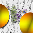
Advanced protein design opens new avenues for nanotechnology
The manufacture of nanoparticles has reached a very high level of control of their shape, size and chemical nature. However, assembling nanoparticles in a controlled manner and with clearly defined functionalities in three-dimensional space remains quite a challenge. Researchers have now taken a first step towards the goal of protein-driven assembly of nanoparticles. In this ground-breaking work, they show that gold nanoparticles with a diameter of 10nm can be assembled using two different protein pairs.
March 8, 2016
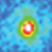
Inorganic perovskite quantum dots for lighting and displays
Luminescent quantum dots (LQDs), which possess high photoluminescence quantum yields, flexible emission color controlling, and solution processibility, are promising for applications in lighting systems (warm white light without UV and infrared irradiation) and high quality displays. However, the commercialization of LQDs has been held back by the prohibitively high cost of their production. In a breakthrough approach, researchers have now succeeded in preparing highly emissive inorganic perovskite quantum dots at room temperature.
March 7, 2016
Writing nanotubes with a nano fountain pen
In new work, an international team of researchers describes the drawing and Raman characterization procedure developed for placing single-walled carbon nanotubes (SWCNTs), proof of SWCNT alignment, optimization of the drawing parameters, and the subsequent placement in predefined lithographic structures for the demonstration of electrical conductivity. In essence, the team developed a simple nanopen for drawing and placing aligned single or multiple rod like molecules nanometrically.
March 2, 2016

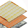
Nanotechnology in textiles - the new black
Nanoengineered functional textiles are going to revolutionize the clothing that you'll wear. The potential of nanotechnology in the development of new materials in the textile industry is considerable. This review discusses electronic and photonic nanotechnologies that are integrated with textiles and shows their applications in displays, sensing, and drug release within the context of performance, durability, and connectivity. On the one hand, existing functionality can be improved using nanotechnology and on the other, it could make possible the manufacture of textiles with entirely new properties or the combination of different functions in one textile material.
February 29, 2016
Self-healing, highly stretchable supercapacitor based on a dual crosslinked polyelectrolyte
Not all electrocapacitive materials are intrinsically stretchable and various modified structures and electron/ion-inactive stretchable substrates have been utilized to introduce stretchability into conventionally rigid supercapacitors. Now, researchers have developed a multifunctional polyelectrolyte, achieving an electrochemically complete self-healability and 600% stretchability of supercapacitors. This work can be applied to other energy conversion and storage devices such as batteries, fuel cells, etc.
February 22, 2016
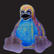
Using household items to make a multi-sensory 'Paper Skin'
Researchers have explored common inexpensive materials to demonstrate their valuable and advantageous properties for artificial skin development. They demonstrate a scalable fabrication approach using off-the-shelf household items such as aluminum foil, scotch tapes, sticky-notes, napkins and sponges to build 'Paper Skin'. Paper Skin promises to be an affordable all-in-one flexibel sensing platform, applicable for applications such as health monitoring, 3D touchscreens, and human-machine interfaces, where sensing diversity, surface adaptability, and large-area mapping all are essential.
February 19, 2016
Nanotechnology for next-generation inkjet color printing
By replacing dye inks with optical nanostructures, researchers have demonstrated the use of inkjet technology to create colored interference layers with high accuracy without the need for high-temperature fixing. The key to this technology is the ability to control the inkjet printing process to form nanostructures with high accuracy. Whereas conventional inkjet printing occurs in the microrange, this new work demonstrates that optical structures can be printed with much greater accuracy, which in particular opens the prospects in developing controlled interference printing of interference color images.
February 11, 2016
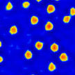
Real-time and label-free detection of single viruses in complex solutions
Many virus detection platforms, including conventional fluorescent label-based ones, have limitations because they are time-intensive and not easily compatible with point-of-care use without the existence of significant infrastructure and expert staff. Researchers have now developed a technique capable of specifically visualizing label-free single viruses in complex solutions in real-time. This approach eliminates virtually all sample preparation.
February 5, 2016