Nanotechnology Spotlight – Latest Articles
 Subscribe to our Nanotechnology Spotlight feed
Showing Spotlights 1913 - 1920 of 3579 in category All (newest first):

Curcumin nanoparticles as innovative antimicrobial and wound healing agents
Researchers have explored the use of curcumin nanoparticles for the treatment of infected burn wounds, an application that resulted in reduced bacterial load and enhancing wound healing. Adding to the excitement regarding curcumin in multiple fields of medicine, most prominently in oncology, these new findings demonstrat that curcumin nanoparticles were more effective at both accelerating thermal burn wound closure and clearing infection with Methicillin Resistant S. aureus (MRSA) as compared to curcumin in its bulk size.
September 22, 2014
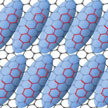
Graphene accelerates the electro-optic response in ferroelectric liquid crystal displays
Ferroelectric liquid crystal (FLC) display technology holds the promise of fast switching times, a large viewing angle, and high resolution. FLCs have a spontaneous polarization whose direction is perpendicular to the layer. This spontaneous polarization plays an imperative role in the electro-optic switching of FLCs. Researchers have now developed a technique to amplify the spontaneous polarization by doping graphene into FLCs.
September 18, 2014
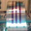
New process allows fully additive roll-to-roll printing of flexible electrochromic devices
Electrochromic devices are some of the most attractive candidates for paper-like displays, so called electronic paper, which will be the next generation display. Researchers have now demonstrated solid state flexible polymer based electrochromic devices are fabricated continuously by stacking layers in one direction. This novel bottom-up approach with no need for a lamination step enables fully printed and 2D patterned organic electrochromics.
September 17, 2014
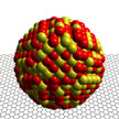
Using microwaves to optimize platinum-nickel nanoalloys for catalytic water treatment
The adoption of a newly developed, facile synthesis method in catalyst designs may permit the rapid screening of nanoalloys for water contaminants. Given the compositional dynamics of this technique, a series of nanoalloys with different surface compositions can be quickly synthesized using a single starting solution and the optimal metal ratio experimentally determined to find the best catalytic reactivity for degrading the pollutant.
September 15, 2014
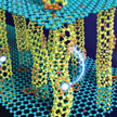
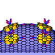
Aligned carbon nanotube/graphene sandwiches for high-rate lithium-sulfur batteries
Researchers consider the rational combination of carbon nanotubes (CNTs) and graphene into three-dimensional hybrids an effective route to amplify the inherent physical properties at the macroscale. By in situ nitrogen doping and structural hybridization of carbon nanotubes and graphene, researchers have now successfully fabricated nitrogen-doped aligned carbon nanotube/graphene sandwiches. In this work, aligned CNTs and graphene layers were anchored to each other, constructing a sandwich-like hierarchical architecture with efficient 3D electron transfer pathways and ion diffusion channels.
September 12, 2014
Flexible high-performance FinFETs with a bending radius of 0.5 mm
The flexibility required when fabricating flexible electronic components has led to the use of plastic substrates and different transfer techniques to fabricate flexible devices. However, one of the biggest obstacles to mass adoption of flexible electronics has been the incompatibility with industry's state-of-the-art silicon-based CMOS processes. Researchers have now developed a new process that can be used to reduce the thickness of the silicon substrate until the required flexibility is obtained. In new work, they demonstrate a flexible (0.5 mm bending radius) nanoscale FinFET on silicon-on-insulator using a back-etch based substrate thinning process.
September 9, 2014
Multimodal graphene biosensor integrates optical, electrical, and mechanical signals
As a prime example of how the integration of multiple disparate nanotechnology fields allows the realization of novel or expanded functionalities, researchers have demonstrated a multimodal sensing device which integrates the functionalities of three traditional single mode sensors. Specifically, the team fabricated a graphene-based multimodal biosensing device, capable of transducing protein binding events into optical, electrical, and mechanical signals.
September 8, 2014
Titania nanotubes' role in building ultrafast rechargeable Li-ion batteries
Nanotechnology has the potential to deliver the next generation lithium-ion batteries (LIBs) with improved performance, durability and safety at an acceptable cost. However, several challenging bottlenecks remain to build the ideal nanostructured electrodes for ultrafast rechargeable LIBs. To overcome these challenges, researchers developed a mechanical force-driven method to prepare elongated bending titania-based nanotubes for high-rate LIBs.
September 4, 2014