Nanotechnology Spotlight – Latest Articles
 Subscribe to our Nanotechnology Spotlight feed
Showing Spotlights 1905 - 1912 of 3579 in category All (newest first):
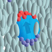
Cleansing the ionic impurities in LCDs with nanoparticles
Impurities during the production process of liquid crystal devices result in mobile ions that influence the LCs' field-induced switching phenomena, resulting in a phenomenon called image sticking, or ghosting. Researchers now have developed a method to reduce the presence of excess ions by doping LCDs with ferroelectric nanoparticles. They demonstrate that this reduction of free ions has coherent impacts on the LC's conductivity, rotational viscosity, and electric field-induced nematic switching.
October 16, 2014
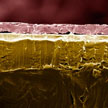
Graphene laminate drastically changes heat conduction of plastic materials
Graphene laminate - multilayer stacks of graphene layers piled on top of each other - is a promising material for thermal coating applications. Researchers have investigated thermal conductivity of graphene laminate films deposited on PET substrates. They found that the compressed laminates have higher thermal conductivity for the same average flake size owing to better flake alignment. This shows a possibility of up to 600-times enhancement of the thermal conductivity of plastic materials by coating them with the thin graphene laminate films.
October 14, 2014
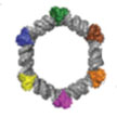
Multifunctional RNA nanoparticles to combat cancer and viral infections
There is a significant need for new therapeutic approaches to combat diseases such as cancer and viral infections. Using RNA as a therapeutic modality brings to bear an entirely new approach, which not only allows for the construction of uniform scaffolds for attachment of functional entities, but also permits the use of all the different types of functionalities that are inherent in natural RNAs. New research demonstrates that multifunctional RNA nanoparticles with a nanoring design allow the use of different types of functionalities inherent in natural RNAs.
October 13, 2014
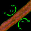
CNT@NCNT coaxial nanocables - Toward full exposure of 'active sites'
Researchers have demonstrated a unique coaxial carbon nanocable material with pristine carbon nanotubes as the core and nitrogen-doped wrinkled carbon layer as the shell. The active sites rendered by the surface enriched dopant atoms on the carbon nanocables are accessible and effective to catalyze the oxygen involved electrochemical reactions. These coaxial nanocables afford higher ORR/OER current compared with the routine bulk doped nitrogen-doped carbon nanotubes.
October 10, 2014

Graphene materials for energy storage applications
Graphene and graphene-based materials have attracted great attention in energy storage applications for batteries and supercapacitors owing to their unique properties of high mechanical flexibility, large surface area, chemical stability, superior electric and thermal conductivities that render them great choices as alternative electrode materials for electrochemical energy storage systems. A recent review article summarizes the progress in graphene and graphene-based materials for four energy storage systems, i.e., lithium-ion batteries, supercapacitors, lithium-sulfur batteries and lithium-air batteries.
October 9, 2014

Nanotechnology compendium for teachers and educators
The European Commission has published a compendium 'Nanotechnologies: Principles, Applications, Implications and Hands-on Activities' that has been specifically developed to provide the educational communities with relevant, accurate and updated materials to inform, motivate and inspire young people to know more about nanosciences and nanotechnologies concepts and applications. This resource has been developed within the context of the European research project Nanoyou, and it has been enriched with numerous and multifaceted inputs, reflections and insights on societal issues, also provided by the European project TimeforNano.
October 6, 2014
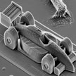
Nanotechnology and 3D-printing
3D-printing processes are engineered to use material more efficiently, give designs more flexibility and produce objects more precisely. These 3D printing techniques are reaching a stage where desired products and structures can be made independent of the complexity of their shapes. Applying 3D printing concepts to nanotechnology could bring similar advantages to nanofabrication - speed, less waste, economic viability - than it is expected to bring to manufacturing technologies. here we show examples of current research into 3D printing in nanotechnology.
September 26, 2014
Healing electronics with light
As we are moving into an era of flexible and wearable electronic devices, one challenge that arises is an increased vulnerability to mechanical failure. Relatively small damages such as tiny cracks along the electrical conductive pathway caused by the bending, twisting and folding of such devices could easily cause the entire gadget to fail. Researchers have now demonstrated light-powered healing of an electrical conductor. They show that green light even with low intensity has potential to provide fast and repetitive recovery of a damaged electrical conductor without any direct invasion.
September 24, 2014