Nanotechnology Spotlight – Latest Articles
 Subscribe to our Nanotechnology Spotlight feed
Showing Spotlights 1897 - 1904 of 3579 in category All (newest first):
2D molybdenum disulfide: a promising new optical material for ultra-fast photonics
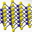
Molybdenum disulfide's (MoS2) semiconducting ability, strong light-matter interaction and similarity to graphene makes it of interest to scientists as a viable alternative in the manufacture of electronics, particularly photoelectronics. In pushing towards practical optical applications of two-dimensional (2D) MoS2, an essential gap on understanding the nonlinear optical response of 2D MoS2 and how it interacts with light, must be filled.
October 30, 2014
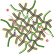
A nano-thermodynamic look at gold-copper alloys
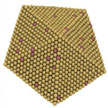
Gold-copper alloys are very popular catalysts in nanotechnology, for instance to efficiently convert carbon dioxide or to help fabricate a more powerful and longer lasting fuel cell material. This alloy exhibits novel physical and chemical properties at the nanoscale. Although the Au-Cu alloy has been extensively studied in the literature both at the bulk and nanoscales, the prediction of phase diagrams at the nanoscale has been missing. A new paper present sthe phase diagram of Au-Cu at the nanoscale for the relevant distinct polyhedral morphologies of nanoparticles at sizes 4 nm and 10 nm.
October 29, 2014
A nanorobotics platform for nanomanufacturing
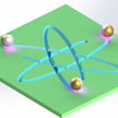
The complexity and high cost of the state-of-the-art high-resolution lithographic systems are prompting unconventional routes for nanoscale manufacturing. Inspired by natural nanomachines, synthetic nanorobots have recently demonstrated remarkable performance and functionality. Nanoengineers now have invented a new nano-patterning approach, named Nanomotor Lithography, which translates the autonomous movement trajectories of nanomotors, or nanorobots, into controlled surface features that brings a twist to conventional static optical fabrication systems.
October 28, 2014
Direct chemical contrast in STM imaging becomes available with new technique
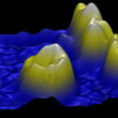
Researchers have demonstrated a new imaging technique that is a marriage between two powerful methods and it promises simultaneous spatial and elemental information of the samples down to the atomic scale. By combining scanning tunneling microscopy (STM) with synchrotron X-ray microscopy, there is now an instrument (SX-STM) that has the potential to perform all the applications of STM and X-rays in a single setting at the ultimate atomic limit.
October 27, 2014

A nanoparticle-based alternative to Viagra
The majority of men who undergo radical prostatectomy for the treatment of prostate cancer will suffer from erectile dysfunction due to disruption of the cavernous nerve. This nerve has been identified as responsible for penile erection. The oral erectogenic PDE5 inhibitors like Viagra rely on the functioning of this nerve to provide the initial burst of nitric oxide necessary to initiate an erection. In this condition nanotechnology - in the form of a nanoparticle delivery system - may come to the rescue by targetting useful therapeutics for penile rehabilitation following radical prostatectomy.
October 24, 2014

Graphene-based biomimetic soft robotics platform
Among the various robotic actuation mechanisms driven by different stimuli, light-driven systems have garnered more and more attention due to their advantages in wireless/remote control, localized rather than whole-field driven capabilities, and electrical/mechanical decoupling. Inspired by the photothermal effect of graphene in biomedical applications, researchers have now demonstrated an easily fabricated and remote/wireless control light-driven approach to actuation mechanism based on graphene nanocomposites.
October 23, 2014

Ultra-stretchable silicon for flexible electronics (w/video)
Researchers have demonstrated ultra-stretchability in monolithic single-crystal silicon. The design is based on an all silicon-based network of hexagonal islands connected through spiral springs. The resulting single-spiral structures can be stretched to a ratio more than 1000%, while remaining below a 1.2% strain. Moreover, these network structures have demonstrated area expansions as high as 30 folds in arrays. This method could provide ultra-stretchable and adaptable electronic systems for distributed network of high-performance macro-electronics especially useful for wearable electronics and bio-integrated devices.
October 21, 2014
Carbon-nanotube paper electrodes with very high loading for lithium-sulfur batteries
Researchers have created a free-standing carbon nanotube paper electrode with high sulfur loading for lithium-sulfur batteries employing a bottom-up strategy to design and fabricate a hierarchical structure. This new fabrication method does not employ aluminum foil or binders, thereby fully utilizing the advantage of a Li-S system with high specific capacity. This proof-of-concept experiment indicates that the rational design of the nanostructured electrode offers the possibility to efficiently use the active materials at practical loading.
October 17, 2014